Eureka AIR delivers breakthrough ideas for toughest innovation challenges, trusted by R&D personnel around the world.

Gold finger manufacturing method and gold finger

A manufacturing method and gold finger technology, which is applied in the direction of printed circuit manufacturing, electrical connection printed components, printed circuit components, etc., can solve short circuit, lifting and laying on the nearby gold finger 2′, nickel-gold layer hanging nickel And other issues

Active Publication Date: 2016-03-23
NEW FOUNDER HLDG DEV LLC +1
View PDF3 Cites 8 Cited by
  • Summary
  • Abstract
  • Description
  • Claims
  • Application Information

AI Technical Summary

Problems solved by technology

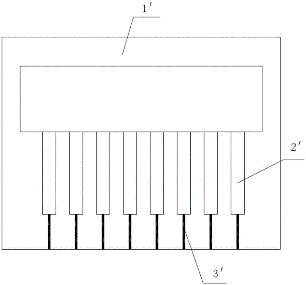
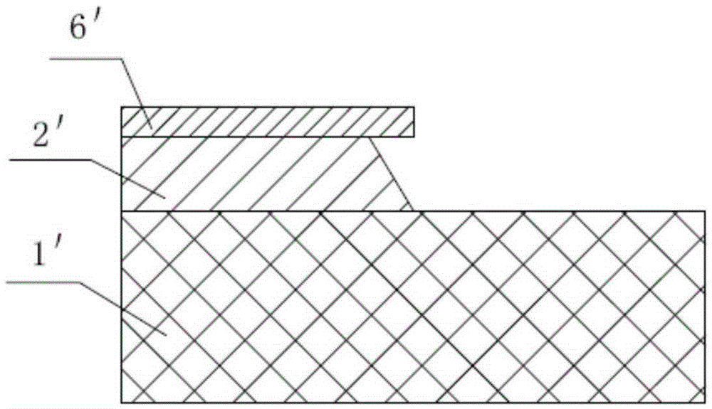
However, in the process of etching, due to the defects of the etching process itself, the phenomenon of side etching will inevitably occur, that is, as the depth increases, the part that starts to be etched is etched for a long time, and the depth of etching to both sides is also large. Furthermore, the nickel-gold layer 6' protruding from the end of the gold finger appears to be a hanging nickel problem
During the process of plugging and unplugging, the nickel-gold layer 6' at the nickel-hanging position will lift up and touch the nearby gold finger 2' due to the problem of nickel suspension at the end of the gold finger after processing the finished gold finger on the client side. phenomenon, resulting in a short circuit

Method used


Image

  • Gold finger manufacturing method and gold finger
  • Gold finger manufacturing method and gold finger
  • Gold finger manufacturing method and gold finger

Examples


Embodiment 1

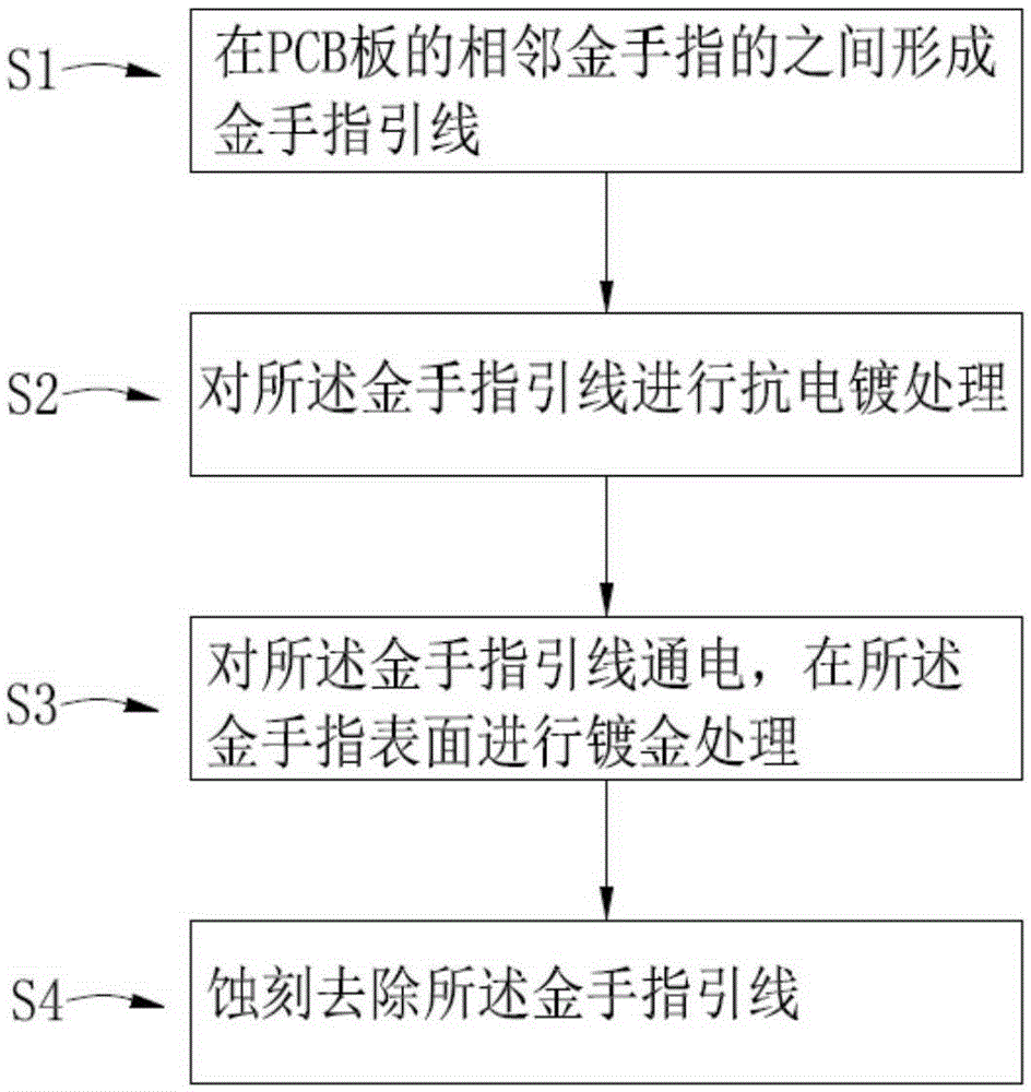
[0040] Such as image 3 As shown, the manufacturing method of a golden finger provided in this embodiment mainly includes the following steps:

[0041] S1: A gold finger lead 3 is formed between adjacent gold fingers 2 on the PCB, wherein the gold finger lead is connected between the root areas of adjacent gold fingers, such as Figure 4 shown;

[0042] S2: Perform anti-plating treatment on the gold finger guide wire 3, such as Figure 5 shown;

[0043] S3: energize the gold finger lead 3, and perform gold plating on the surface of the gold finger 2;

[0044] S4: Etching and removing the gold finger wire 3 .

[0045] It should be noted that the root area of ​​the gold finger refers to the area away from the end (ie, the free end, the end for plugging) of the gold finger.

[0046]In the manufacturing method of the above gold finger, the gold finger guide line 3 is arranged between the sides of the adjacent gold finger 2, and when the gold finger guide line 3 is etched afte...

Embodiment 2

[0054] This embodiment provides a gold finger, which is prepared by any one of the manufacturing methods described in Embodiment 1.

[0055] Since the nickel-gold layer 6 is still electroplated on the end of the above-mentioned gold finger and there is no hanging nickel phenomenon, when the client is plugged and used, the nickel-gold layer 6 at the end of the gold finger is prevented from being tilted to the adjacent gold finger. cause a short circuit. Therefore, the stability of the structure and function of the product is guaranteed when it is used.


PUM


Abstract

The invention provides a gold finger manufacturing method and a gold finger. The gold finger manufacturing method comprises: forming a gold finger index wire between adjacent gold fingers on a PCB; performing anti-electroplating treatment on the gold finger index wire; electrifying the gold finger index wire, and performing gold plating treatment on the surface of a gold finger; and etching to remove the gold finger index wire. According to the manufacturing method, the gold finger index wire is manufactured between adjacent gold fingers; when gold plating treatment is completed and the gold finger index wire is etched, lateral erosion appears on the side of a gold finger, and the rear end of the gold finger is still electroplated with a nickel-gold layer, and does not generate suspended nickel; and moreover, the gold finger is plugged at a client, avoiding the short circuit defect caused when the nickel-gold layer at the rear end of the gold finger is jointed to adjacent gold fingers, and thereby guaranteeing the structure and function stability of a prepared product.

Description

technical field [0001] The invention relates to the field of printed circuit boards, in particular to a gold finger manufacturing method and the gold finger. Background technique [0002] On the printed circuit board near the edge of the board, there are many rectangular metal contacts arranged in rows, and the metal contacts are formed by electroplating a layer of nickel gold on the copper surface of the printed circuit board. These metal contacts are part of the printed circuit board and are called gold fingers because of their nickel-gold-plated surface and their shape resembling fingers. Gold fingers are used for connection between printed circuit boards, capable of connecting circuits and transmitting signals. The nickel-gold layer on the surface of the gold finger can improve the insertion resistance, conductivity and oxidation resistance of this part. Cheats are generally divided into equal-length cheats, graded cheats and segmented cheats. The design of graded and ...

Claims


Application Information

Patent Timeline
IPC IPC(8): H05K1/11H05K3/40
CPCH05K1/117H05K3/403H05K2201/09727H05K2203/304
Inventor 李俊
Owner NEW FOUNDER HLDG DEV LLC
Why Eureka
Eureka Blog
Learn More