
Etching method of thick copper circuit board

A circuit board and etching technology, which is applied to the etching field of thick copper circuit boards, can solve the problems that affect the productivity and output of the etching production line, affect the quality and production efficiency of other boards, and cannot be completely eliminated, so as to improve the etching efficiency and reduce the cost. , the effect of reducing the line width difference

Active Publication Date: 2019-03-08
SHENZHEN WUZHU TECH
View PDF3 Cites 0 Cited by
  • Summary
  • Abstract
  • Description
  • Claims
  • Application Information

AI Technical Summary

Problems solved by technology

[0009] 1. The difference in line width between the upper and lower boards during etching is mainly caused by the pool effect of the upper and lower boards. This effect cannot be completely eliminated by adjusting the etching spray pressure on the upper and lower sides of the etching cylinder. The difference in line width between the upper and lower boards after etching It still exists, especially for thick copper circuit boards;
[0010] 2. Frequent adjustment of the pressure of the etching cylinder will affect the quality and production efficiency of other boards, and affect the production capacity and output of the entire etching production line

Method used


Image

  • Etching method of thick copper circuit board
  • Etching method of thick copper circuit board
  • Etching method of thick copper circuit board

Examples


Embodiment Construction

[0029] The present invention will be further described below in conjunction with the accompanying drawings and embodiments.

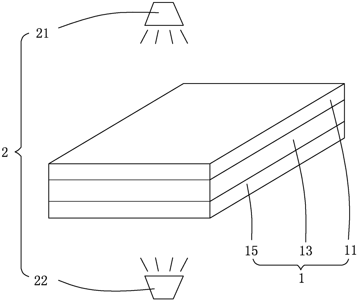
[0030] see figure 1 , is a schematic diagram of etching a thick copper circuit board in the method for etching a thick copper circuit board of the present invention. The thick copper circuit board 1 includes a top copper layer 11 , a substrate 13 and a bottom copper layer 15 . The top copper layer 11 and the bottom copper layer 15 are respectively disposed on two sides of the substrate 13 .

[0031] The top copper layer 11 and the bottom copper layer 15 are thick copper foil, and the thickness of the thick copper foil is above 2OZ.

[0032] The etching production line for the etching process includes a film stripping station, an etching station, a tin stripping station, a turning device (not shown) and a return device (not shown). The thick copper circuit board 1 is transported horizontally along the etching production line, and passes through the st...


PUM


Abstract

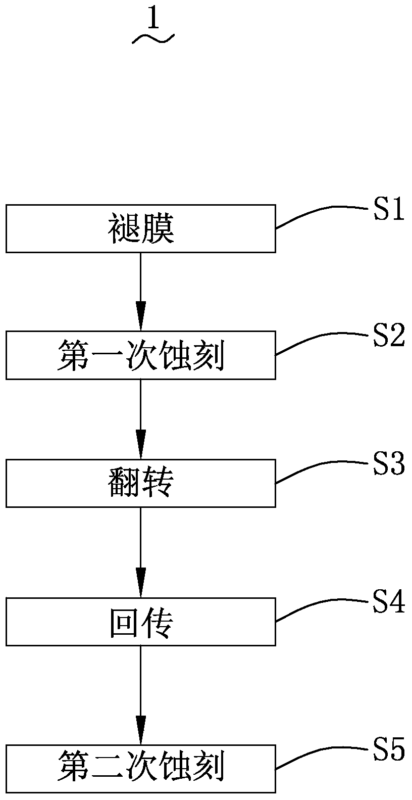
The invention provides an etching method of a thick-copper circuit board. The etching method of the thick-copper circuit board comprises film stripping, first etching, overturn, postback, second etching and other steps. Compared with correlation technologies, the etching method of the thick-copper circuit board can effectively reduce a two-face etching line width difference, and the etching method of the thick-copper circuit board is low in cost.

Description

technical field [0001] The invention relates to the technical field of circuit board processing, in particular to an etching method for a thick copper circuit board. Background technique [0002] The thickness of the copper layer covering both sides of the printed circuit board is usually HOZ (half ounce, half ounce, 1OZ=28.35g) or 1OZ (ounce, ounce). With the rapid development of electronic technology, thick copper (the thickness of the copper layer is more than 2OZ ) The demand for circuit boards has increased sharply. Thick copper circuit boards play an important role in high-current substrates and have the following advantages: [0003] 1. It can transfer the heat generated by the components to the outside of the substrate, so it can realize the purpose of high-density interconnection of high-power electrical appliances; [0004] 2. In the application fields of automobiles, power supplies, electric power and electronics, thick copper foil high-current substrates are use...

Claims


Application Information

Patent Timeline
Patent Type & Authority Patents(China)
IPC IPC(8): H05K3/06
CPCH05K3/068H05K2203/1476
Inventor 朱占植蔡志浩邵勇陈家刚
Owner SHENZHEN WUZHU TECH
Learn More