LGP (light guide plate) and manufacture method thereof, array substrate and manufacture method thereof and a display device
A technology of an array substrate and a manufacturing method, applied in the display field, can solve the problems of lowering the brightness of the display area, lowering the pixel transmittance, lowering the pixel aperture ratio, etc., so as to reduce the brightness difference, weaken the brightness difference line, and achieve uniform display brightness. Effect
- Summary
- Abstract
- Description
- Claims
- Application Information
AI Technical Summary
Problems solved by technology
Method used
Image
Examples
Embodiment 1
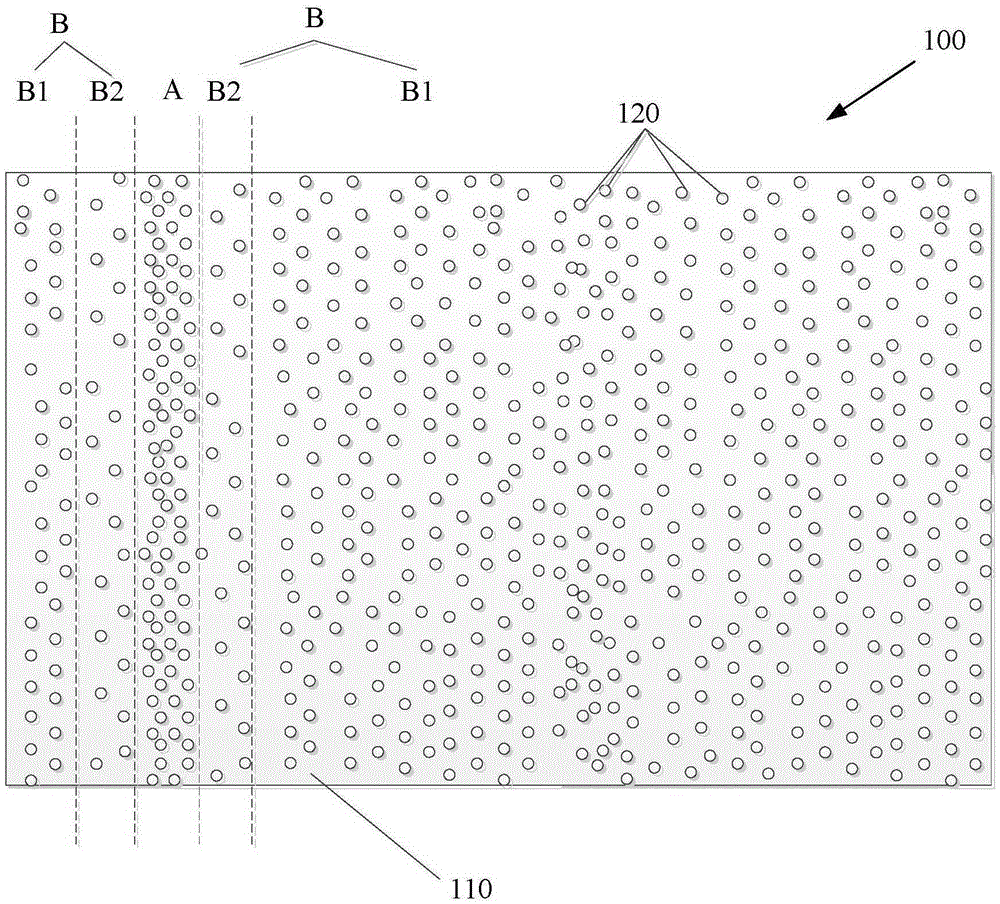
[0030] Embodiment 1 of the present invention provides a light guide plate, see figure 1 with image 3 The light guide plate body 110 of the light guide plate 100 is provided with a plurality of dots 120, wherein the density of the dots 120 in the first area A of the light guide body 110 is greater than that of the dots 120 in the second area B of the light guide body 110 density.
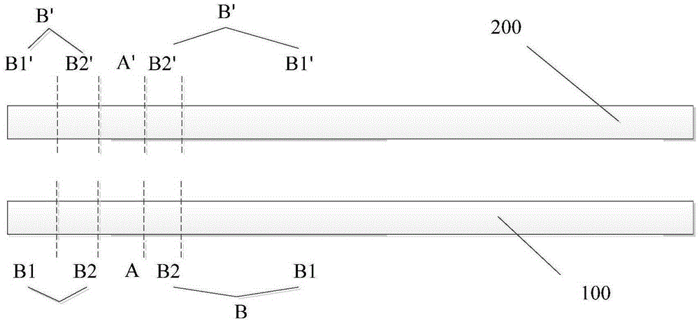
[0031] The first area A here is the area corresponding to the first display area A' of the array substrate 200 when the light guide plate main body 110 is applied to a display device, and the first display area A' here is the pixel unit on the array substrate The display area in which the gate drive circuit is made; the second area B here is the area outside the first area A, corresponding to the second display area B', and the second display area B' here is the first display area A ' outside the area.
[0032] Since the density of the grid dots 120 in the first area A is greater than the density...
Embodiment 2
[0037] Embodiment 2 of the present invention provides a light guide plate, see figure 2 with image 3The light guide plate body 110 of the light guide plate 100 is provided with a plurality of dots 120, wherein the diameter of the dots 120 in the first region A of the light guide body 110 is larger than that of the dots 120 in the second region B of the light guide body 110 diameter.
[0038] The first area A here is the area corresponding to the first display area A' of the array substrate 200 when the light guide plate main body 110 is applied to a display device, and the first display area A' here is the area on the array substrate 200. The display area where the gate drive circuit is made in the pixel unit; the second area B here is the area outside the first area A, corresponding to the second display area B, and the second display area B' here is the first display area Area outside of A'.
[0039] Since the diameter of the grid dots 120 in the first area A is larger ...
Embodiment 3
[0047] Embodiment 3 of the present invention provides an array substrate, see Figure 4 , the array substrate is a GIA array substrate, which can be divided into a first display area A' and a second display area B', wherein the second display area B' includes a first sub-display area B1' and a second sub-display area B2', The length of the pixel electrode P in the column direction in the second sub-display area B2' is smaller than the length of the pixel electrode P in the column direction in the first sub-display area B1', and the length of the pixel electrode P in the second sub-display area B2' The length in the row direction is the same as the length in the row direction of the pixel electrode P in the first sub-display area B1'; wherein, the first display area A' is a display area in which a gate driving circuit is fabricated in the pixel unit, and the second The display area B' is an area outside the first display area A', and the second sub-display area B2' is located b...
PUM
 Abstract
Description
Claims
Application Information
 - R&D
- Intellectual Property
- Life Sciences
- Materials
- Tech Scout
- Unparalleled Data Quality
- Higher Quality Content
- 60% Fewer Hallucinations
Browse by: Latest US Patents, China's latest patents, Technical Efficacy Thesaurus, Application Domain, Technology Topic, Popular Technical Reports.
© 2025 PatSnap. All rights reserved.Legal|Privacy policy|Modern Slavery Act Transparency Statement|Sitemap|About US| Contact US: help@patsnap.com


