Ferroelectric-semiconductor pn junction type novel laminated solar cell
A stacked sun and pn junction technology, applied in the field of solar energy and solar cells, can solve the problem of small short-circuit current
- Summary
- Abstract
- Description
- Claims
- Application Information
AI Technical Summary
Problems solved by technology
Method used
Image
Examples
Embodiment
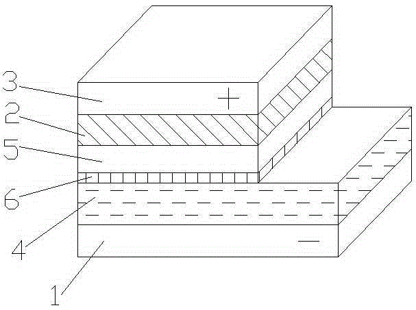
[0062] The stacked solar cell in the embodiment of the present invention includes a metal electrode, a substrate pn junction, an inorganic ferroelectric material layer, and a transparent oxide electrode, and the metal electrode, the substrate pn junction, the inorganic ferroelectric material layer, and the transparent oxide electrode are connected in sequence , the substrate pn junction is located between the metal electrode and the inorganic ferroelectric material layer, and the inorganic ferroelectric material layer is located between the substrate pn junction and the transparent oxide electrode. Wherein, the substrate pn junction is located above the metal electrode, the inorganic ferroelectric material layer is located above the substrate pn junction, and the transparent oxide electrode is located above the inorganic ferroelectric material layer. Meanwhile, in some embodiments of the present invention, a transition layer is also provided between the substrate pn junction an...
PUM
| Property | Measurement | Unit |
|---|---|---|
| Thickness | aaaaa | aaaaa |
| Thickness | aaaaa | aaaaa |
| Thickness | aaaaa | aaaaa |
Abstract
Description
Claims
Application Information
 - R&D
- Intellectual Property
- Life Sciences
- Materials
- Tech Scout
- Unparalleled Data Quality
- Higher Quality Content
- 60% Fewer Hallucinations
Browse by: Latest US Patents, China's latest patents, Technical Efficacy Thesaurus, Application Domain, Technology Topic, Popular Technical Reports.
© 2025 PatSnap. All rights reserved.Legal|Privacy policy|Modern Slavery Act Transparency Statement|Sitemap|About US| Contact US: help@patsnap.com


