


Quick Research
Generate reliable direction feasibility study reports for your R&D in just a few steps.

Technical Q&A
Discover and master advanced knowledge NOW. Basics, ideas, possibilities, all at once.

Find Solutions
As an expert in R&D theories, this can generate solutions to your technical problems instantly.

Evaluate Feasibility
Analyze your overall solution with one click, know your potential R&D risks in advance.

Monitor Landscape
Get weekly tech updates, stay abreast of the latest tech innovations and key insights.
Amorphous silicon germanium thin-film solar cell having double-layer interface band gap buffer layer
A solar cell, amorphous silicon thin film technology, applied in circuits, photovoltaic power generation, electrical components, etc., can solve problems such as serious interface recombination, and achieve the effects of enhancing absorption, reducing recombination, and facilitating transmission
- Summary
- Abstract
- Description
- Claims
- Application Information
AI Technical Summary
Problems solved by technology
Method used
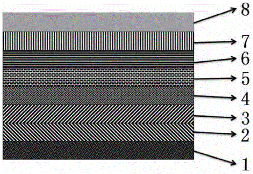
Image

Examples
Embodiment 1
[0036] In this embodiment, an amorphous silicon germanium thin-film solar cell with a flexible substrate having a continuously changing bandgap absorbing layer and a double-layer interfacial bandgap buffer layer is prepared according to the following steps:
[0037] (1) Select a mirror-finished stainless steel strip with a thickness of 100 μm and a surface roughness of 3 nm as the substrate, and clean it. The cleaning process is: ultrasonic cleaning with deionized water, acetone, and ethanol for 20 minutes in sequence.
[0038] (2) The bottom electrode of the battery was prepared by magnetron sputtering: a 300nm thick Ag layer and a 200nm thick AZO layer were sequentially prepared on the substrate, and the radio frequency power was 100w and 200w respectively. The transmittance of AZO in the visible light range is 60% to 80%, and the resistivity of AZO is 8.5×10 -3 Ω·cm.
[0039] (3) Chemically treat the Ag / AZO to form a micro-nano structure on the base surface. The method i...
Embodiment 2
[0048] In this embodiment, an amorphous silicon germanium thin-film solar cell with a flexible substrate having a continuously changing bandgap absorbing layer and a double-layer interface bandgap buffer layer is prepared according to the following steps:
[0049] (1) Float glass with a thickness of 100 μm and a surface roughness of 2 nm is selected as a substrate and cleaned. The cleaning process is: ultrasonic cleaning with deionized water, acetone, and ethanol for 20 minutes in sequence.
[0050] (2) Prepare the bottom electrode of the battery by magnetron sputtering method: prepare a 400nm thick AZO layer on the substrate, the purpose is to transmit light from the front and back directions, and the radio frequency power is 200w respectively. The transmittance of AZO in the visible light range is 60% to 80%, and the resistivity of AZO is 8.5×10 -3 Ω·cm.
[0051] (3) AZO is chemically treated to form a micro-nano structure on the base surface. The method is to wash with h...
PUM
 Abstract
Description
Claims
Application Information
 - R&D Engineer
- R&D Manager
- IP Professional
- Industry Leading Data Capabilities
- Powerful AI technology
- Patent DNA Extraction
Browse by: Latest US Patents, China's latest patents, Technical Efficacy Thesaurus, Application Domain, Technology Topic, Popular Technical Reports.
© 2024 PatSnap. All rights reserved.Legal|Privacy policy|Modern Slavery Act Transparency Statement|Sitemap|About US| Contact US: help@patsnap.com