


Quick Research
Generate reliable direction feasibility study reports for your R&D in just a few steps.

Technical Q&A
Discover and master advanced knowledge NOW. Basics, ideas, possibilities, all at once.

Find Solutions
As an expert in R&D theories, this can generate solutions to your technical problems instantly.

Evaluate Feasibility
Analyze your overall solution with one click, know your potential R&D risks in advance.

Monitor Landscape
Get weekly tech updates, stay abreast of the latest tech innovations and key insights.
Wafer test result comparison method and wafer test result comparison system
A technology for wafer testing and test results, which is applied in semiconductor/solid-state device testing/measurement, special data processing applications, instruments, etc. It can solve the problems of poor efficiency, low accuracy of manual comparison, and inability to automatically compare wafer test results and other issues to achieve the effect of improving accuracy and efficiency
- Summary
- Abstract
- Description
- Claims
- Application Information
AI Technical Summary
Problems solved by technology
Method used
Image


Examples
Embodiment 1
[0051] An embodiment of the present invention provides a method for comparing wafer test results, which is used to realize automatic comparison of wafer test results, so as to improve comparison efficiency and accuracy.
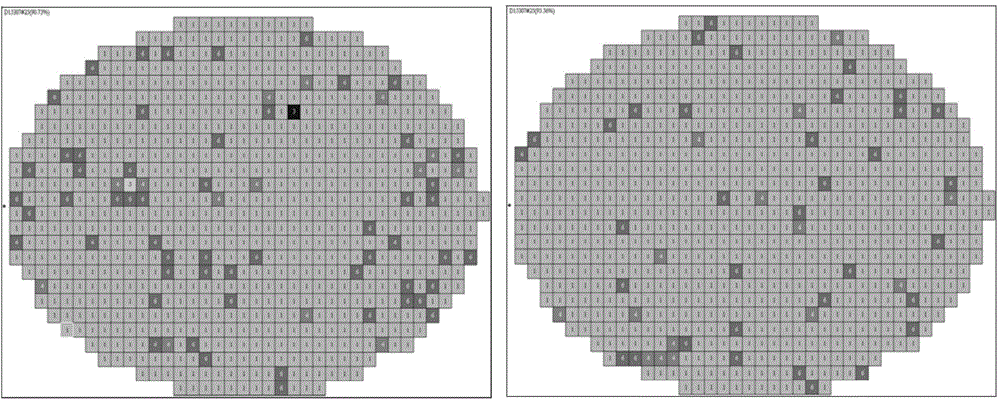
[0052] Below, refer to Figure 4The wafer test result comparison method proposed by the embodiment of the present invention will be described. Figure 4 It is a flow chart of a method for comparing wafer test results in an embodiment of the present invention.
[0053] The wafer test result comparison method of the present embodiment comprises the following steps:
[0054] Step A1: Obtain the first set of wafer test results and the second set of wafer test results.
[0055] Wherein, the first group of wafer test results and the second group of wafer test results can be obtained through the wafer probe test, or the first group of wafer test results and the second group of wafer test results can be directly read from the storage device. result.
[0056] The ...
Embodiment 2
[0085] An embodiment of the present invention provides a wafer test result comparison system, which can be used to implement the wafer test result comparison method described in the first embodiment.
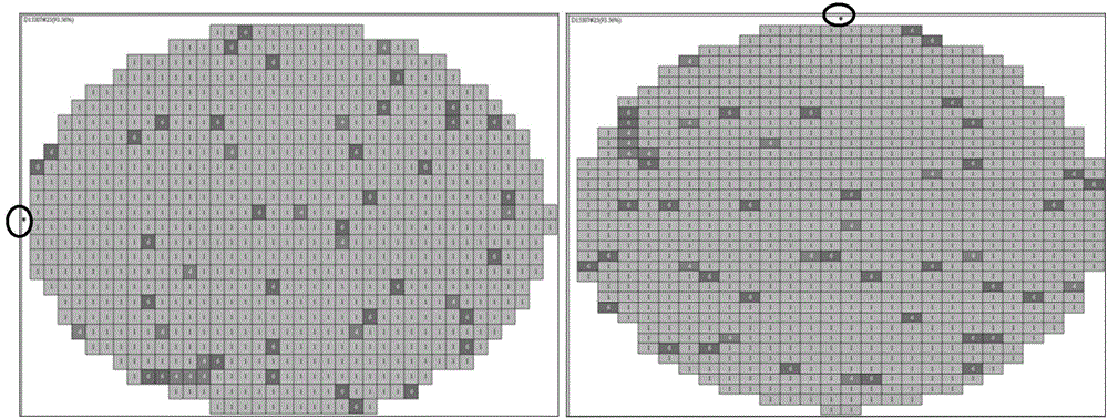
[0086] like Figure 5 As shown, the wafer test result comparison system of the present embodiment includes:
[0087] Wafer test result acquisition unit 501, configured to acquire the first set of wafer test results and the second set of wafer test results;
[0088] A file format parsing unit 502, configured to parse the first set of wafer test results and the second set of wafer test results into the first set of test result analysis data and the second set of test result analysis data;
[0089] The wafer angle and coordinate adjustment unit 503 is used to judge whether the wafer angle and coordinates of the first set of test result analysis data and the second set of test result analysis data match. The second set of test result analysis data is adjusted to match the wafer an...
PUM
 Abstract
Description
Claims
Application Information
 - R&D Engineer
- R&D Manager
- IP Professional
- Industry Leading Data Capabilities
- Powerful AI technology
- Patent DNA Extraction
Browse by: Latest US Patents, China's latest patents, Technical Efficacy Thesaurus, Application Domain, Technology Topic, Popular Technical Reports.
© 2024 PatSnap. All rights reserved.Legal|Privacy policy|Modern Slavery Act Transparency Statement|Sitemap|About US| Contact US: help@patsnap.com