Formation method of PMOS transistor

A technology of transistors and semiconductors, applied in semiconductor/solid-state device manufacturing, electrical components, circuits, etc., can solve problems such as sufficient stress applied to the channel region, poor performance of PMOS transistors, etc., to improve hole mobility and improve performance Effect

Pending Publication Date: 2015-12-30
SEMICON MFG INT (SHANGHAI) CORP
View PDF13 Cites 1 Cited by
  • Summary
  • Abstract
  • Description
  • Claims
  • Application Information

AI Technical Summary

Problems solved by technology

However, in the PMOS transistor formed by the existing method, the formed epitaxial silicon germanium layer 103 is too far away from the channel region, and the distance between the two is usually as Figure 4 The distance D1 shown i

Method used


Image

  • Formation method of PMOS transistor
  • Formation method of PMOS transistor
  • Formation method of PMOS transistor

Examples


Embodiment Construction

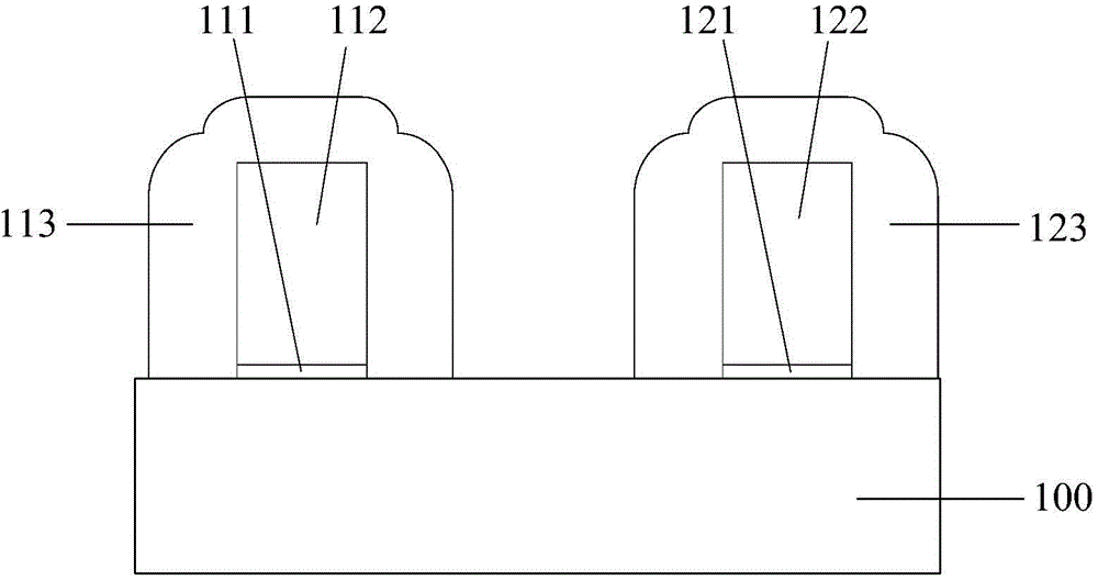
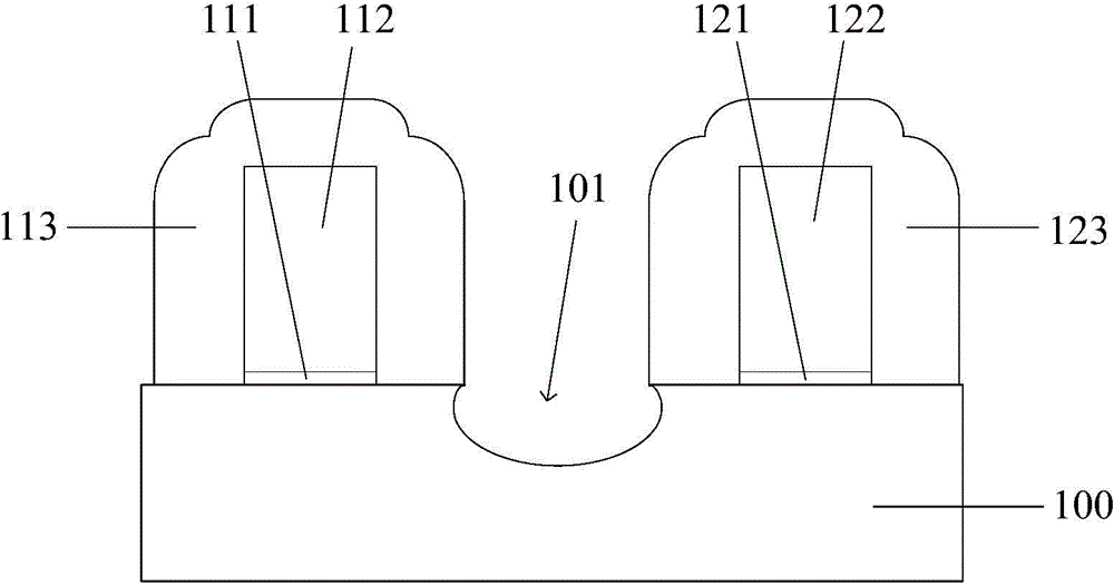
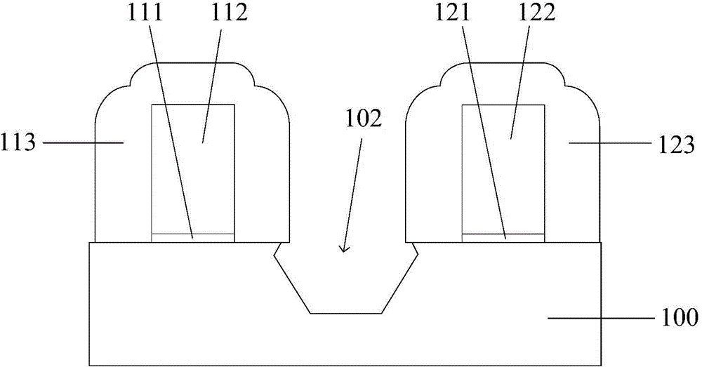
[0035] As mentioned in the background, in the existing PMOS transistors, the epitaxial silicon germanium layer is too far away from the channel region, so sufficient stress cannot be applied to the channel region, and the performance of the PMOS transistor is not good. Further analysis shows that this is because the thickness of the sidewall formed by the existing PMOS transistor formation method is relatively large, and when the groove is formed by a dry etching process, the distance from the sidewall of the groove to the channel region is relatively long. The distance between the epitaxial silicon germanium layer that subsequently fills the groove and the channel region is relatively long, therefore, the epitaxial silicon germanium layer cannot act well on the channel region.

[0036] For this reason, the present invention provides a new method for forming a PMOS transistor. The method first forms a first groove, then forms a depression on the side wall of the first groove, a...


PUM


Abstract

The invention relates to a formation method of a PMOS transistor. The formation method includes the following steps that: a semiconductor substrate is provided, and the surface of the semiconductor substrate is provided with a plurality of discrete gate structures; one first side wall is formed on the upper surface and two sides of each gate structure; the semiconductor substrate under adjacent first side walls is oxidized, so that an oxide layer is formed; a second side wall covering the first side wall is formed at the upper surface and two sides of each gate structure, the total thickness of the first side wall and the second side wall is the thickness of a target side wall; the oxide layer and the semiconductor substrate below the oxide layer are etched, so that a first groove can be formed; the residual of the oxide layer is removed until recesses formed at the side walls of the groove; the semiconductor substrate between the recessed side walls and the bottom of the groove are removed through etching until a second Sigma-shaped groove can be formed; and a silicon germanium layer is formed in the second groove. The performance of the PMOS transistor formed by the formation method is improved.

Description

technical field [0001] The invention relates to the field of semiconductor manufacturing, in particular to a method for forming a PMOS transistor. Background technique [0002] In the existing manufacturing process of semiconductor devices, since stress can change the energy gap and carrier mobility of silicon materials, improving the performance of MOS transistors through stress has become an increasingly common technical means. Specifically, by properly controlling the stress, the mobility of carriers (electrons in NMOS transistors and holes in PMOS transistors) can be increased, thereby increasing the driving current, thereby greatly improving the performance of MOS transistors. [0003] At present, Embedded SiGe Technology is usually used to form the source and drain regions of PMOS transistors, that is, silicon germanium materials are formed in the regions where the source and drain regions need to be formed, and then doped to form the source regions of PMOS transistors...

Claims


Application Information

Patent Timeline
IPC IPC(8): H01L21/336
Inventor 刘佳磊
Owner SEMICON MFG INT (SHANGHAI) CORP
Why Eureka
Try Eureka