A method of forming a field stop layer in a semiconductor device
A field stop layer, semiconductor technology, applied in the direction of semiconductor devices, semiconductor/solid state device manufacturing, electrical components, etc., can solve the problems of inability to use, field stop layer limitation, high injection dose, etc., to avoid the influence of the front structure of the device. Effect
- Summary
- Abstract
- Description
- Claims
- Application Information
AI Technical Summary
Problems solved by technology
Method used
Image
Examples
Embodiment 1
[0041] A method of forming a field stop layer in a semiconductor device, comprising the steps of:
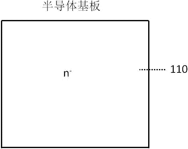
[0042] A) A semiconductor device is selected, including a semiconductor substrate 110 of the first conductivity type.
[0043] B) Proton implantation is performed from the back surface of the semiconductor substrate 110 of the first conductivity type of the semiconductor device described in A), and the implantation process is completed.
[0044] C) After the implantation process in step B), the semiconductor device is annealed in an annealing device, so as to form a first semiconductor region 111 a with a concentration higher than that of the semiconductor substrate 110 of the first conductivity type.
[0045] The depth of the first semiconductor region 111a formed in C) from the back surface of the semiconductor device is d 1 .
[0046]The thickness of the first semiconductor region 111a formed in C) is h 1 .
[0047] D) Perform ion implantation from the back surface of the...
Embodiment 2
[0055] A method of forming a field stop layer in a semiconductor device, comprising the steps of:
[0056] A) A semiconductor device is selected, including a semiconductor substrate 110 of the first conductivity type. The first conductivity type in A) is n-type.
[0057] B) Proton implantation is performed from the back surface of the semiconductor substrate 110 of the first conductivity type of the semiconductor device described in A), and the implantation process is completed. The proton injection dose described in B) is 1e 12 cm -2 ~1e 16 cm -2 , the injection energy is 300KeV~6MeV.
[0058] C) After the implantation process in step B), the semiconductor device is annealed in an annealing device, so as to form a first semiconductor region 111 a with a concentration higher than that of the semiconductor substrate 110 of the first conductivity type. The depth of the first semiconductor region 111a formed in C) from the back surface of the semiconductor device is d 1 ...
Embodiment 3
[0063] A method of forming a field stop layer in a semiconductor device, comprising the steps of:
[0064] A) A semiconductor device is selected, including a semiconductor substrate 110 of the first conductivity type. The first conductivity type in A) is n-type.
[0065] B) Proton implantation is performed from the back surface of the semiconductor substrate 110 of the first conductivity type of the semiconductor device described in A), and the implantation process is completed. The proton injection dose described in B) is 1e 14 cm -2 , the injection energy is 2MeV.
[0066] C) After the implantation process in step B), the semiconductor device is annealed in an annealing device, so as to form a first semiconductor region 111 a with a concentration higher than that of the semiconductor substrate 110 of the first conductivity type. The depth of the first semiconductor region 111a formed in C) from the back surface of the semiconductor device is d 1 . The thickness of the...
PUM
 Abstract
Description
Claims
Application Information
 - R&D
- Intellectual Property
- Life Sciences
- Materials
- Tech Scout
- Unparalleled Data Quality
- Higher Quality Content
- 60% Fewer Hallucinations
Browse by: Latest US Patents, China's latest patents, Technical Efficacy Thesaurus, Application Domain, Technology Topic, Popular Technical Reports.
© 2025 PatSnap. All rights reserved.Legal|Privacy policy|Modern Slavery Act Transparency Statement|Sitemap|About US| Contact US: help@patsnap.com


