Manufacturing method of display panel, display panel, and display device
A display panel and display device technology, which is applied in the field of display panel structure, display device, and display panel manufacturing, can solve problems that affect the appearance of the display, and achieve the effect of improving the degree of beautification and realizing narrower borders
- Summary
- Abstract
- Description
- Claims
- Application Information
AI Technical Summary
Problems solved by technology
Method used
Image

Examples
Embodiment 1
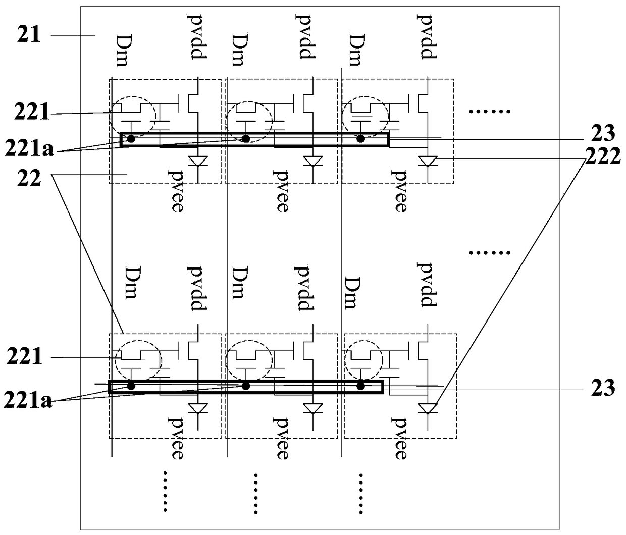
[0027] Figure 2a A schematic structural diagram of a display panel provided in Embodiment 1 of the present invention, as shown in Figure 2a shown, including:
[0028] The substrate 21 can be, for example, a glass substrate.
[0029] The pixel units 22 are arranged and formed on the substrate 21 in a matrix form, as shown in the dotted line box in the figure. Wherein, the pixel unit 22 includes a driving transistor 221 (shown by a dotted ellipse) and an OLED light emitting device 222 , and the driving transistor 221 is used to drive the OLED light emitting device 222 to emit light.
[0030] At least one scanning signal driving circuit 23, such as Figure 2a As shown in the thick black line box of , the scanning signal driving circuit 23 is formed on the substrate 21 , and the scanning signal driving circuit 23 is used to input a scanning signal to the gate 221 a of the driving transistor 221 . In order to realize the narrowing of the display panel and improve the beautifi...
Embodiment 2
[0043] Figure 3a A schematic structural diagram of a display device provided in Embodiment 2 of the present invention, as shown in Figure 3a As shown, the display device 30 specifically includes the display panel 31 described in the above embodiments.
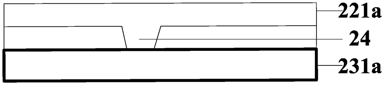
[0044] Specifically, such as Figure 3bAs shown, in the display panel 31 , the scanning signal driving circuit 32 is located below the pixel unit 33 , and an insulating layer 34 is covered between the scanning signal driving circuit 32 and the pixel unit 33 . Wherein, the optional material of the insulating layer 34 is silicon nitride and / or silicon oxide.
[0045] Wherein, the structure of the pixel unit 33 includes a polysilicon layer 331 (for example, it can be formed by low-temperature polysilicon), and a gate insulating layer 332 for isolating the polysilicon layer 331 and the gate 333 (for example, it can be formed by silicon oxide or nitride) from bottom to top. Silicon), gate 333 (for example, formed by metal), int...
Embodiment 3
[0050] Based on the above display panel, this embodiment proposes a method for manufacturing the display panel. Figure 4 A schematic flow chart of a method for manufacturing a display panel provided in Embodiment 3 of the present invention, as shown in Figure 4 shown, including:
[0051] Step 41, forming a scanning signal drive circuit on the substrate by patterning;
[0052] Specifically, a buffer layer, a polysilicon layer, a gate insulating layer, a gate, an interlayer insulating layer, and source and drain electrodes of the scanning signal driving circuit are sequentially formed on the substrate from bottom to top using a patterning process.
[0053] Step 42, covering the scanning signal drive circuit with an insulating layer;
[0054] Specifically, on the basis of the substrate formed in step 41 above, an insulating layer is formed above the source and drain electrodes.
[0055] Step 43, opening a first through hole on the insulating layer, the position of the first ...
PUM
 Abstract
Description
Claims
Application Information
 - R&D
- Intellectual Property
- Life Sciences
- Materials
- Tech Scout
- Unparalleled Data Quality
- Higher Quality Content
- 60% Fewer Hallucinations
Browse by: Latest US Patents, China's latest patents, Technical Efficacy Thesaurus, Application Domain, Technology Topic, Popular Technical Reports.
© 2025 PatSnap. All rights reserved.Legal|Privacy policy|Modern Slavery Act Transparency Statement|Sitemap|About US| Contact US: help@patsnap.com