FPGA-based BiSS-C communication protocol method
A communication protocol and reference clock technology, applied in electrical components, transmission systems, etc., can solve problems such as resource occupation and multi-line delay processing
- Summary
- Abstract
- Description
- Claims
- Application Information
AI Technical Summary
Problems solved by technology
Method used
Image
Examples
specific Embodiment approach 1
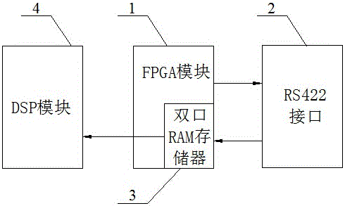
[0012] Specific implementation mode one: combine figure 1 As shown, its method steps are:
[0013] Step 1: The phase-locked loop of FPGA module 1 first generates a 300MHz reference clock. When SLout is idle at a high level, the MA starts to send a clock. According to the 300MHz reference clock, it first delays for a fixed time T1, and the MA clock is always set to 0, and then delays for a fixed time. T2, the MA clock is always set to 1. If the data reception of this bit is completed, restart from the delay fixed time T1 until a frame of data is completely received, and continue to cycle from the first step, thus generating the MA clock signal, the clock signal MA Send to the clock input terminal of the external grating sensor through the RS422 interface 2;
[0014] Step 2: The rising edge of the clock signal MA triggers the data signal transmission of the external grating sensor, the data signal is output through the reading head of the external grating sensor, and transmitte...
PUM
 Abstract
Description
Claims
Application Information
 - R&D
- Intellectual Property
- Life Sciences
- Materials
- Tech Scout
- Unparalleled Data Quality
- Higher Quality Content
- 60% Fewer Hallucinations
Browse by: Latest US Patents, China's latest patents, Technical Efficacy Thesaurus, Application Domain, Technology Topic, Popular Technical Reports.
© 2025 PatSnap. All rights reserved.Legal|Privacy policy|Modern Slavery Act Transparency Statement|Sitemap|About US| Contact US: help@patsnap.com

