Adaptive voltage source, shift register and unit thereof, and display
An adaptive voltage and sensing unit technology, applied in static memory, static indicator, digital memory information, etc., can solve the problems of too fast threshold voltage drift of related TFTs and difficult to extend circuit life, and prevent the threshold voltage from drifting too fast. , the effect of prolonging life
- Summary
- Abstract
- Description
- Claims
- Application Information
AI Technical Summary
Problems solved by technology
Method used
Image

Examples
Embodiment 1
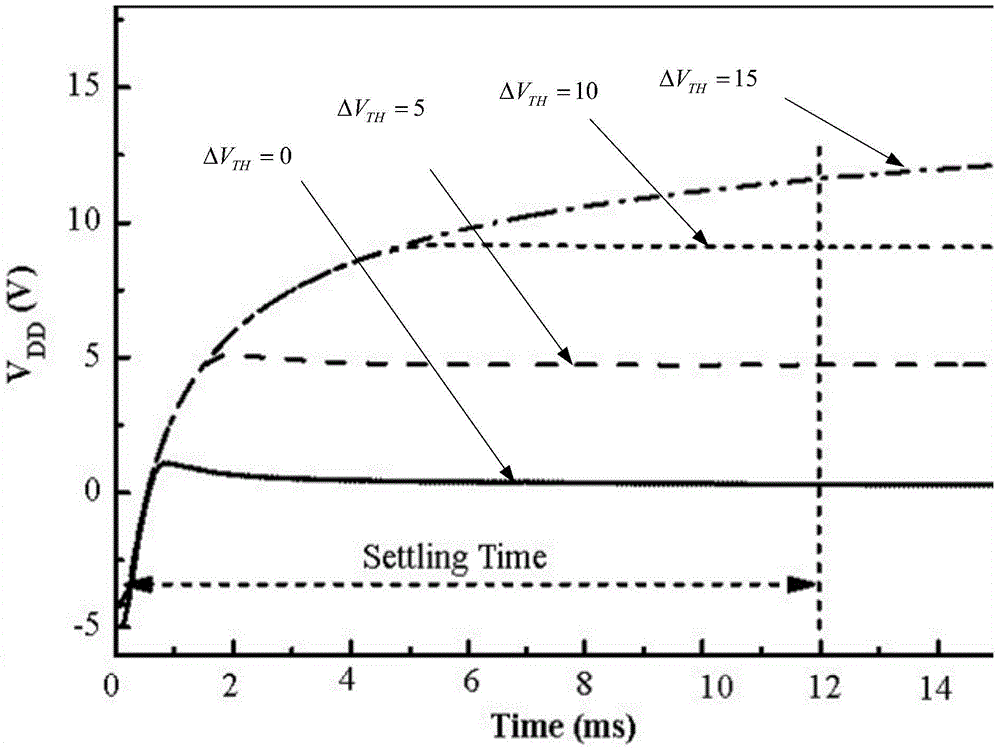
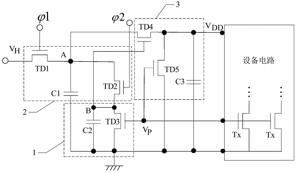
[0050] Please refer to image 3 , is the structural diagram of the self-adaptive voltage source of this embodiment. The adaptive voltage source structure includes: for the voltage source V in series H The sensing module 1 and the reference resistor between the low level end and the low level end form a circuit. Wherein, the sensing module 1 includes a sensing unit TD3, which is preferably a triode. In other embodiments, the sensing unit TD3 may also be composed of other transistors such as diodes by connecting / coupling with other elements to function as a triode. In this embodiment, the sensing unit TD3 is taken as an example of a thin film transistor for illustration. The control electrode (such as the gate) of the sensing unit TD3 is the sensing terminal of the sensing module 1, which is used to be coupled to the transistor Tx to be sensed. In the sensing device circuit The threshold voltage shift of the transistor Tx to be sensed.
[0051] In a specific embodiment, the c...
Embodiment 2
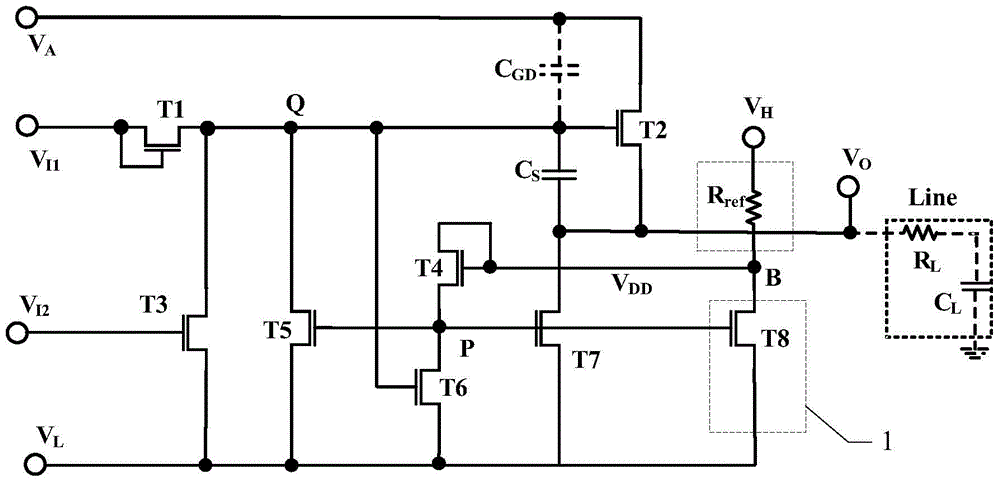
[0073] The adaptive voltage source disclosed in Embodiment 1 is applicable to any device circuit that adjusts the supply voltage based on the threshold voltage of a transistor, and a shift register unit is taken as an example for illustration. Please refer to Figure 7 , is a circuit structure diagram of the shift register unit disclosed in this embodiment. The shift register unit includes: a driving module 20 , an input module 10 , a low level maintaining module 30 and the aforementioned adaptive voltage source 40 . in,
[0074] The driving module 20 is configured to convert the first signal V through the switch state A It is transmitted to the signal output end of the shift register unit, thereby outputting the scan signal. After the drive control terminal Q is charged to obtain the drive voltage, the first signal V A Signal output to the shift register unit. In a specific embodiment, the driving module 20 may include a second transistor T2 for coupling to the signal ou...
PUM
 Abstract
Description
Claims
Application Information
 - R&D Engineer
- R&D Manager
- IP Professional
- Industry Leading Data Capabilities
- Powerful AI technology
- Patent DNA Extraction
Browse by: Latest US Patents, China's latest patents, Technical Efficacy Thesaurus, Application Domain, Technology Topic.
© 2024 PatSnap. All rights reserved.Legal|Privacy policy|Modern Slavery Act Transparency Statement|Sitemap