
BGA package chip test clamp

A technology for testing fixtures and installing chips, which is applied to the casing of measuring devices, etc., can solve problems such as large errors, difficult processing, and high prices, and achieve the effects of simple design, low cost, and high stability

Inactive Publication Date: 2015-11-18
SHENZHEN GONGJIN ELECTRONICS CO LTD
View PDF6 Cites 6 Cited by
  • Summary
  • Abstract
  • Description
  • Claims
  • Application Information

AI Technical Summary

Problems solved by technology

[0004] The purpose of the present invention is to solve the problem that when testing BGA-packaged chips, the test result of the method of reserving test points has a large error with the actual result, and the BG

Method used


Image

  • BGA package chip test clamp
  • BGA package chip test clamp

Examples


Embodiment 1

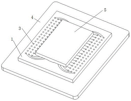
[0019] Example 1, such as figure 1 , figure 2 As shown, this implementation example is a test fixture that adopts the DDRSDRAM test of a BGA package chip. After using this fixture, the DDRSDRAM chip 5 to be tested can be welded, and then welded to the mainboard 4 that uses the DDRSDRAM chip to work normally on the mainboard. , use the test point 3 on the test fixture to test the DDR SDRAM chip that is working normally.

[0020] Such as figure 2 As shown, in the present embodiment, the fixture main body is a fixture plate 1 made of a multilayer printed circuit board, and the top surface and the bottom surface of the fixture plate 1 are all provided with BGA pads consistent with the DDRSDRAM chip 5 pins to be tested 2. The pads 2 on the top surface and the bottom surface are correspondingly connected through the printed circuit board via holes and printed circuit board traces. Like this, when the DDRSDRAM chip 5 to be tested is welded on the pad 2 on the fixture plate 1 top...


PUM


Abstract

The invention provides a BGA package chip test clamp. The test clamp is a clamp plate formed by a plurality of layers of printed-circuit boards. The top surface and the bottom surface of the clamp plate are respectively provided with a BGA bonding pad consistent with pins of a BGA package chip to be tested; the top surface of the clamp plate is provided with test points; the bonding pads on the top surface and the bottom surface of the clamp plate are in wiring communication through printed-circuit board via holes and the printed-circuit boards; when the BGA chip to be tested is packaged on the top surface of the clamp plate, the bottom surface of the clamp plate is packaged on a main board using the BGA chip to be tested; and the test points and signal lines needing testing in the bonding pads are in wiring communication through the printed-circuit boards. According to the BGA package chip test clamp, the test clamp can realize more accurate measurement result, and the cost is low.

Description

technical field [0001] The invention relates to the testing field of BGA packaged chips, in particular to a test fixture used for signal integrity testing of BGA packaged DDR chips. Background technique [0002] BGA was developed in the 1990s with the advancement of integration technology, the improvement of equipment, and the use of deep submicron technology. A new packaging technology has emerged. Chips packaged with BGA technology can make the chip have smaller volume, better electrical performance, faster speed and better heat dissipation performance without changing the function. Now more and more chips are packaged in BGA , such as a DDR SDRAM chip used to store programs and data. DDRSDRAM chips have a wide range of application requirements in embedded devices, portable devices and handheld computers. [0003] For embedded systems, usually in the process of PCB design, testability design is done, that is, which signals are planned to be tested, and then test points ...

Claims


Application Information

Patent Timeline
IPC IPC(8): G01R1/04
Inventor 贺龙胜庞建荣黄玉
Owner SHENZHEN GONGJIN ELECTRONICS CO LTD
Learn More