Two-dimensional planar temperature field test sensing element and manufacturing method thereof
A technology of sensing elements and two-dimensional planes, applied in thermometers, thermometers, thermometers with electric/magnetic elements that are directly sensitive to heat, etc., can solve problems such as object structure disturbances, affecting the accuracy of temperature field testing, etc., to achieve The effect of large test range, convenient production, and high temperature sensitivity
- Summary
- Abstract
- Description
- Claims
- Application Information
AI Technical Summary
Problems solved by technology
Method used
Image
Examples
Embodiment 1
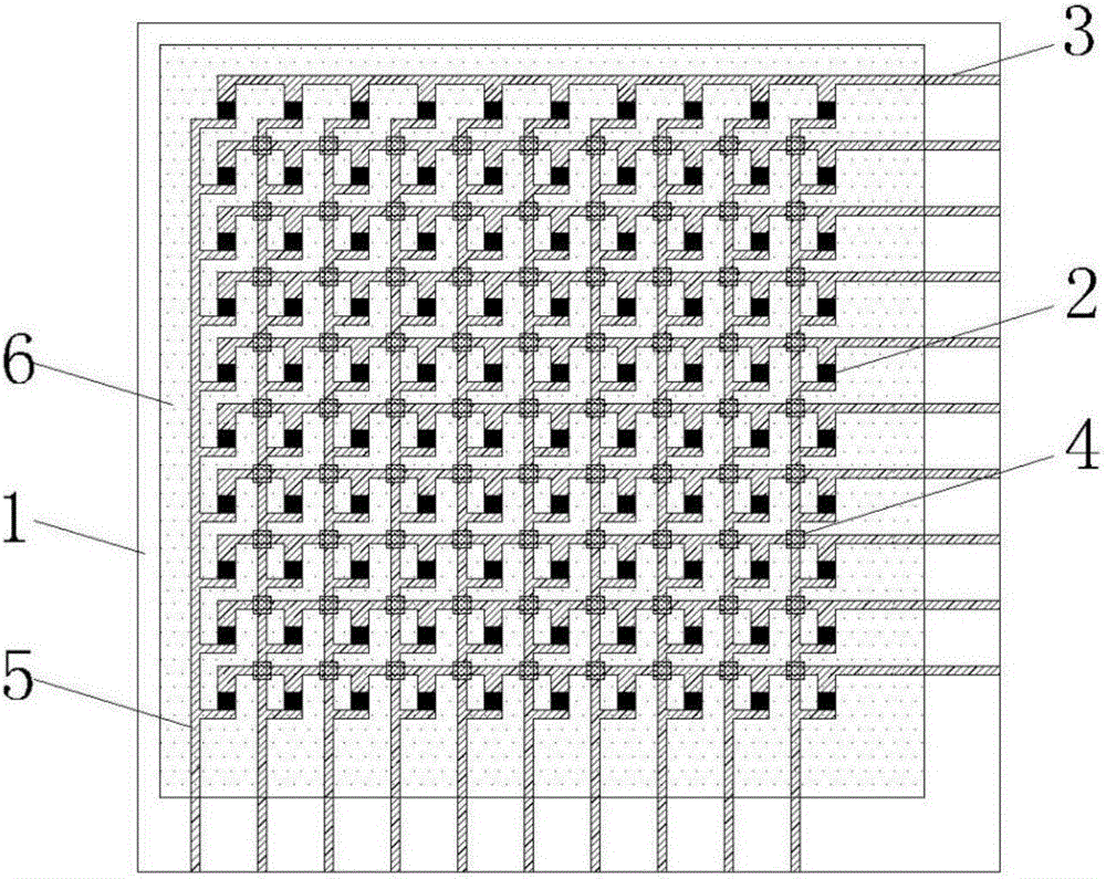
[0025] Embodiment 1: as figure 1 Shown, a kind of two-dimensional plane temperature field test sensing element of the present invention, it is made of the thin film 1 of the first layer, the sensitive element display 2 of the second layer and lateral electrode 3, the insulating thin layer 4 of the third layer, the first layer It consists of four layers of vertical electrodes 5 and a fifth layer of insulating protective film 6 . For example, a polyimide film with a relatively large temperature tolerance range is selected as the film 1 of the first layer, and the thickness of the film 1 is selected to be 0.1 mm. The sensitive element display 2 of the second layer uses epoxy resin as a matrix and conductive carbon black as a filling material to prepare a conductive polymer composite material, and then prints it on the film 1; before printing, the upper surface of the film 1 is scrubbed clean with a solvent, Guaranteed printing effect. The lateral electrodes 3 of the second laye...
Embodiment 2
[0027] Embodiment 2: as figure 1Shown, a kind of two-dimensional plane temperature field test sensing element of the present invention, it is made of the thin film 1 of the first layer, the sensitive element display 2 of the second layer and lateral electrode 3, the insulating thin layer 4 of the third layer, the first layer It consists of four layers of vertical electrodes 5 and a fifth layer of insulating protective film 6 . For example, a polyimide film with a relatively large temperature tolerance range is selected as the film 1 of the first layer, and the thickness of the film 1 is selected to be 0.1 mm. The sensitive element display 2 of the second layer uses epoxy resin as the matrix and carbon nanotubes as the filling material to prepare a conductive polymer composite material, and then prints on the film 1; before printing, the upper surface of the film 1 is cleaned with a solvent, Guaranteed printing effect. The lateral electrodes 3 of the second layer are also pri...
PUM
| Property | Measurement | Unit |
|---|---|---|
| Thickness | aaaaa | aaaaa |
Abstract
Description
Claims
Application Information
 - R&D
- Intellectual Property
- Life Sciences
- Materials
- Tech Scout
- Unparalleled Data Quality
- Higher Quality Content
- 60% Fewer Hallucinations
Browse by: Latest US Patents, China's latest patents, Technical Efficacy Thesaurus, Application Domain, Technology Topic, Popular Technical Reports.
© 2025 PatSnap. All rights reserved.Legal|Privacy policy|Modern Slavery Act Transparency Statement|Sitemap|About US| Contact US: help@patsnap.com


