Semiconductor annealing method utilizing a vacuum environment

A vacuum environment and semiconductor technology, applied in semiconductor/solid-state device manufacturing, semiconductor/solid-state device testing/measurement, electrical components, etc., can solve problems such as difficult environmental control

Active Publication Date: 2015-09-16
TAIWAN SEMICON MFG CO LTD
View PDF4 Cites 5 Cited by
  • Summary
  • Abstract
  • Description
  • Claims
  • Application Information

AI Technical Summary

Problems solved by technology

However, the residual O 2 still have some level of influence
At the same time, consistent environmental control, including chamber matching, is difficult

Method used


Image

  • Semiconductor annealing method utilizing a vacuum environment
  • Semiconductor annealing method utilizing a vacuum environment
  • Semiconductor annealing method utilizing a vacuum environment

Examples


Embodiment Construction

[0030] The following disclosure of the invention provides many different embodiments or examples for implementing different features of different embodiments. Specific examples of components and arrangements are described below to simplify the present disclosure. Of course, this is just an example and is not intended to limit the present invention. Additionally, the invention may repeat reference numerals and / or characters in multiple instances. This repetition is for simplicity and clarity, and does not in itself indicate a relationship between the various embodiments and / or configurations described.

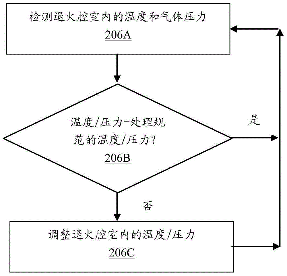
[0031] As described herein, exemplary embodiments of the present invention utilize a vacuum environment to eliminate and / or mitigate problems caused by anneal chamber gases during the anneal process. In a generalized embodiment, a semiconductor annealing system includes an annealing chamber, a heating element, and a vacuum pump connected to the annealing chamber to establish ...


PUM


Abstract

A semiconductor annealing method and system uses a vacuum pump to produce a vacuum environment in the annealing chamber to thereby remove undesired gas element influences. A control system obtains pressure and temperature measurements from the annealing chamber to control operation of the heating elements and vacuum pump to thereby maintain process integrity.

Description

[0001] Cross References to Related Applications [0002] This application claims the invention of U.S. Nonprovisional Patent Application No. Priority No. 61 / 779,424, the entire contents of which are hereby incorporated by reference. technical field [0003] The present invention generally relates to the technical field of semiconductors, and more specifically, relates to a semiconductor annealing method utilizing a vacuum environment. Background technique [0004] Various annealing methods (spike annealing, spike annealing, millisecond annealing, etc.) have been developed for different purposes. However, all these methods have their disadvantages. For advanced technologies, the focus is not only on thermal control, but also on the management of the chamber environment. Existing annealing methods all have gas (O 2 , N 2 or other gases). Therefore, the presence of environmental control and particulate problems will adversely affect the annealing process. For sub-second ...

Claims


Application Information

Patent Timeline
Patent Type & Authority Applications(China)
IPC IPC(8): H01L21/02H01L21/66
CPCH01L21/67017H01L21/324H01L21/67248H01L21/67115H01L21/67253
Inventor 詹尊仁吕政达曾立德陈奕翰陈明德
Owner TAIWAN SEMICON MFG CO LTD
Why Eureka
Try Eureka