
A kind of preparation method of light-emitting diode that improves leakage current

A technology of light-emitting diodes and leakage current, applied in circuits, electrical components, coatings, etc., can solve problems such as crystal growth defects, adverse effects on the performance or function of the latter layer, reverse leakage of light-emitting diode structures, etc., to increase the carrier gas. flow, improve reliability, and reduce the effect of reverse leakage current

Active Publication Date: 2018-07-10
ANHUI SANAN OPTOELECTRONICS CO LTD
View PDF4 Cites 0 Cited by
  • Summary
  • Abstract
  • Description
  • Claims
  • Application Information

AI Technical Summary

Problems solved by technology

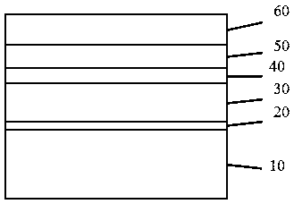
At present, the main blue and green light-emitting devices are nitride semiconductors, see figure 1 , the existing conventional epitaxial structure is substrate 10, buffer layer 20, N-type layer 30, shallow quantum well layer 40, quantum well layer 50 and P-type layer 60, and due to the environment The conditions are very sensitive, so if the chamber environment is not changed to the growth of the next layer in time after the growth of the previous layer is over during the growth process, it is easy to cause adverse effects on the performance or function of the latter layer, such as N-type layer and Shallow quantum well layer, since the N-type layer is a high-concentration doped layer, its doping concentration is more than 10 times higher than the set concentration of impurities in the shallow quantum well layer, when the N-type layer growth is completed, when the shallow quantum well layer continues to grow , the impurities remaining in the N-type layer grow into the shallow quantum well layer, causing defects during crystal growth, and then the reverse leakage phenomenon of the light-emitting diode structure occurs.
[0003] In normal products, if the light-emitting diode structure works at 5V voltage and 20mA current, the leakage current should be zero under ideal conditions, but this is not the case in reality. Due to the limitation of actual growth conditions, leakage current will generally occur. This situation limits The photoelectric performance and service conditions of the light-emitting diode structure are greatly reduced, and the service performance and anti-light decay performance of the light-emitting diode are greatly reduced.
In the existing manufacturing technology, it often occurs that the reverse leakage current of the light-emitting diode exceeds 1μA or even 10μA when it works at 5V voltage and 20mA current, which greatly reduces the reliability of the light-emitting diode structure and the yield rate of production.

Method used


Image

  • A kind of preparation method of light-emitting diode that improves leakage current
  • A kind of preparation method of light-emitting diode that improves leakage current
  • A kind of preparation method of light-emitting diode that improves leakage current

Examples


Embodiment 1

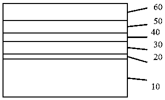
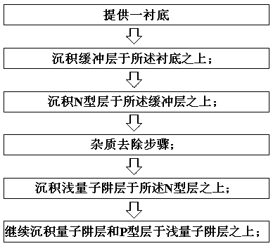
[0031] See attached figure 2 and 3 , a light-emitting diode preparation method for improving leakage current, comprising the following processes:

[0032] First provide the substrate 10, put it into the MOCVD chamber, the material of the substrate 10 is sapphire, silicon, silicon carbide, etc., the sapphire substrate is preferred here; adjust the temperature of the MOCVD chamber to 400~1200°C, and feed the metal source (gallium source is preferred here), NH 3 、H 2 Perform epitaxial growth of a buffer layer 20 with a thickness of 10-3000 nm, and cover the surface of the substrate 10; adjust the temperature of the chamber to 900-1200 ° C, in the above metal source, NH 3 、H 2 Under the condition of continuous feeding, increase the feeding of N-type impurities to grow the N-type layer 30 with a thickness of 4-6 μm. The impurities are selected from one of silicon, germanium or tin. In this embodiment, silicon impurities are preferred. , the impurity concentration is 1×10 17 ...


PUM


Abstract

The invention proposes a method for preparing a light-emitting diode. An impurity removal step is inserted between the deposition steps of the N-type layer and the shallow quantum well layer, and the carrier gas flow rate of the impurity pipeline is increased by using a steep change method, and the pipeline is fully and quickly purged. The remaining impurities can prevent the residual impurities from entering the shallow quantum well layer to affect the crystal structure of the layer, reduce the impact on the reverse leakage current of the light-emitting diode, and improve the reliability of the LED structure and the yield rate of production.

Description

technical field [0001] The invention relates to the technical field of light-emitting diode preparation, in particular to a preparation method of a light-emitting diode with improved leakage current. Background technique [0002] Light-emitting diodes have the advantages of energy saving, environmental protection, and long life, and have been widely used in LCD backlights, outdoor displays, landscape lighting, and general lighting. At present, the main blue and green light-emitting devices are nitride semiconductors, see figure 1 , the existing conventional epitaxial structure is substrate 10, buffer layer 20, N-type layer 30, shallow quantum well layer 40, quantum well layer 50 and P-type layer 60, and due to the environment The conditions are very sensitive, so if the chamber environment is not changed to the growth of the next layer in time after the growth of the previous layer is over during the growth process, it is easy to cause adverse effects on the performance or ...

Claims


Application Information

Patent Timeline
Patent Type & Authority Patents(China)
IPC IPC(8): C23C16/44H01L33/00
Inventor 林继宏卓昌正林兓兓张家宏
Owner ANHUI SANAN OPTOELECTRONICS CO LTD
Learn More