Semiconductor optical detector

A photodetector and semiconductor technology, applied in semiconductor devices, electric solid state devices, and photometry using electric radiation detectors, etc., can solve problems such as difficulty in photographing subjects in real time.

Active Publication Date: 2015-09-02
PANASONIC INTPROP MANAGEMENT CO LTD
View PDF6 Cites 16 Cited by
  • Summary
  • Abstract
  • Description
  • Claims
  • Application Information

AI Technical Summary

Problems solved by technology

Therefore, it is difficult to capture the subject in real time

Method used


Image

  • Semiconductor optical detector
  • Semiconductor optical detector
  • Semiconductor optical detector

Examples


no. 1 Embodiment approach

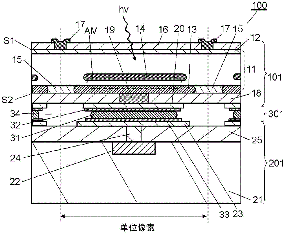
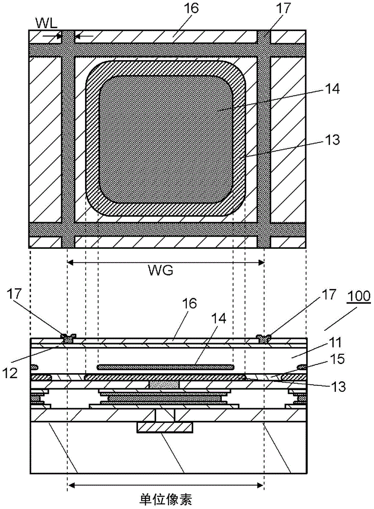
[0044] First, refer to figure 1 and figure 2 The structure of the unit pixel of the semiconductor photodetector according to the first embodiment of the present invention will be described. also, figure 2 In order to clearly show the arrangement of the semiconductor photodetector according to this embodiment in plan view, a partial perspective view is used. In addition, in this specification, "planar view" means viewing from the normal direction of the light receiving surface of the photoelectric conversion part 101 .

[0045] In the semiconductor photodetector 100 according to this embodiment, a plurality of unit pixels are arranged in a matrix on the semiconductor substrate 21 . Each of the plurality of unit pixels has a photoelectric conversion unit 101 and a detection circuit unit 201 , and the photoelectric conversion unit 101 and the detection circuit unit 201 are electrically connected by a junction 301 .

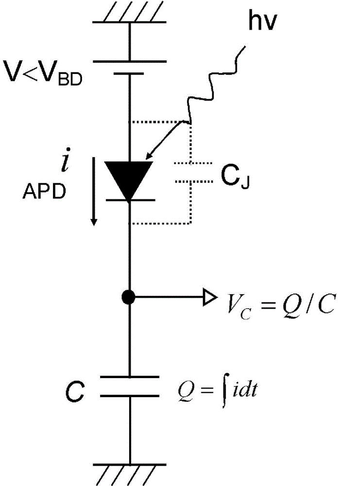
[0046] First, the photoelectric conversion unit 101 will ...

no. 2 Embodiment approach

[0132] Below, refer to Figure 13 and Figure 14 , the structure of the unit pixel of the semiconductor photodetector 500 according to the second embodiment of the present invention will be described.

[0133] In the semiconductor photodetector 500 according to this embodiment, a plurality of unit pixels are arranged in a matrix on a semiconductor substrate 516 . Each of the plurality of unit pixels has a photoelectric conversion unit 502 and a detection circuit unit 504 , and the photoelectric conversion unit 502 and the detection circuit unit 504 are electrically connected via a pixel electrode 506 and a contact plug 514 .

[0134] The photoelectric conversion unit 502 is constituted by a semiconductor unit 508 formed of a photoconductive material. An electrode 510 is formed on the incident-side surface of the semiconductor portion 508 .

[0135] Examples of photoconductive materials include Se-containing semiconductors, compound semiconductors CuIn x Ga 1-x S y Se 1-...


PUM

PropertyMeasurementUnit
melting pointaaaaaaaaaa

Abstract

Provided is a semiconductor optical detector that is capable of detecting weak light including random light by significantly reducing dark-time noise and multiplicative noise from those in conventional semiconductor optical detectors. This semiconductor optical detector has at least one unit pixel having a photoelectric conversion section, a charge storage section, and a detecting circuit. The charge storage section photoelectrically converts inputted light, and has a charge multiplying region where charges are multiplied by means of avalanche multiplication. The charge storage section is connected to the photoelectric conversion section, and stores signal charges transmitted from the photoelectric conversion section. The detecting circuit is connected to the charge storage section, converts the signal charges stored in the charge storage section into voltage, amplifies the voltage by means of an amplifying section, and outputs the amplified voltage.

Description

technical field [0001] The invention relates to a semiconductor photodetector, in particular to a semiconductor photodetector for detecting weak light. Background technique [0002] In recent years, in various fields such as medical treatment, biology, and radiation measurement, photodetectors that accurately measure even weak light of 1 photon are required. Currently, a photomultiplier tube (Photomultiplier Tube: PMT) is widely used as a photodetector for detecting weak light. However, since a PMT as a vacuum tube device has a minimum size of about 10 mm x 10 mm, it is difficult to multi-pixel. In addition, in order to perform two-dimensional imaging using the PMT, it is necessary to scan the object in the XY plane, collect information on each point of the object, and then image it. Therefore, it is difficult to capture a subject in real time. Among them, in order to simultaneously increase the number of pixels and increase the speed of a photodetector that detects weak ...

Claims


Application Information

Patent Timeline
Patent Type & Authority Applications(China)
IPC IPC(8): H01L27/146G01J1/42G01T1/20H01L31/02H04N5/369
CPCG01J1/44H01L27/14665H04N5/369H01L27/14623H01L27/14634H01L27/14609H04N5/37455H01L2924/381H01L27/14612H04N25/60H04N25/63H04N25/772H04N25/70H04N25/75H01L31/107
Inventor 薄田学广濑裕加藤刚久寺西信一
Owner PANASONIC INTPROP MANAGEMENT CO LTD
Why Eureka
Try Eureka