A device for realizing the conversion between space wave and terahertz artificial surface plasmon wave
An artificial surface plasmon and space wave technology, applied in the direction of electrical components, optical components, waveguide devices, etc., can solve the problems that limit the development and application of terahertz SSPP devices, low efficiency, etc., and achieve light weight, good application prospects, small size effect
- Summary
- Abstract
- Description
- Claims
- Application Information
AI Technical Summary
Problems solved by technology
Method used
Image
Examples
example 1
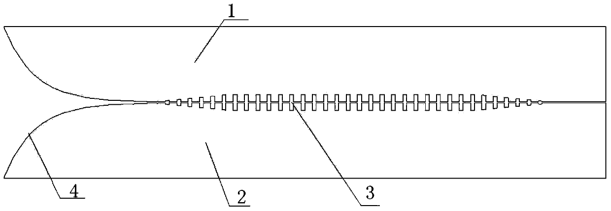
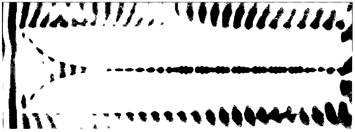
[0024] like figure 2 As shown, on the low-loss flexible Rogers 5880 dielectric substrate, the metal slotted structure is prepared by microlithography, and the unit size is as follows: the horizontal period of the structure p = 75um; the vertical width of the structure is 1412um; the width of the middle slot is 12um; The defects in the structure are 25um wide and 50um high. The corresponding exponential function equation of the first metal sheet is: Where d=1976um, h=812um, s=12um, c=3. . The second metal sheet is symmetrical to the first metal sheet about the x-axis. The simulation results of the CST Microwave Studio show (the monitoring frequency is 0.6THz, and the distance between the monitoring position and the structure surface is 15 microns), when the terahertz plane wave is incident along the horizontal direction, the SPP wave can be effectively excited.
example 2
[0026] like image 3 As shown, on the low-loss flexible Rogers 5880 dielectric substrate, the metal slotted structure is prepared by microlithography, and the unit size is as follows: the horizontal period of the structure p = 75um; the vertical width of the structure is 1412um; the width of the middle slot is 12um; The defects in the structure are 25um wide and 50um high. The corresponding exponential function equation of the first metal sheet is: Where d=1976um, h=812um, s=12um, c=3. The second metal sheet is symmetrical to the first metal sheet about the x-axis. The simulation results of CST Microwave Studio show (the monitoring frequency is 0.6THz, and the distance between the monitoring position and the structure surface is 15 microns), when the plane wave is incident along the oblique direction, that is, when the incident surface is in the x-y plane and the electric field has both x and y direction components (incident The angle θ is 45°), the structure can still rea...
example 3
[0028] like Figure 4 As shown, on the low-loss flexible Rogers 5880 dielectric substrate, the metal slotted structure is prepared by microlithography, and the unit size is as follows: the horizontal period of the structure p = 75um; the vertical width of the structure is 1412um; the width of the middle slot is 12um; The defects in the structure are 25um wide and 50um high. The corresponding exponential function equation of the first metal sheet is: Where d=1976um, h=812um, s=12um, c=3. . The second metal sheet is symmetrical to the first metal sheet about the x-axis. The simulation results of the CST microwave studio show (the monitoring frequency is 0.6THz, and the distance between the monitoring position and the surface of the structure is 15 microns), when the incident surface is on the x-z plane (incident angle φ is 45°), and the electric field is along the y direction, the structure can also Accepts plane waves and converts them to SPP waves.
[0029] It can be see...
PUM
 Abstract
Description
Claims
Application Information
 - R&D Engineer
- R&D Manager
- IP Professional
- Industry Leading Data Capabilities
- Powerful AI technology
- Patent DNA Extraction
Browse by: Latest US Patents, China's latest patents, Technical Efficacy Thesaurus, Application Domain, Technology Topic, Popular Technical Reports.
© 2024 PatSnap. All rights reserved.Legal|Privacy policy|Modern Slavery Act Transparency Statement|Sitemap|About US| Contact US: help@patsnap.com


