Pixel driving circuit, driving method thereof, array substrate and display device
一种像素驱动电路、驱动周期的技术,应用在显示装置,像素驱动电路及其驱动方法,阵列基板领域,能够解决驱动方法复杂、功耗高等问题
- Summary
- Abstract
- Description
- Claims
- Application Information
AI Technical Summary
Problems solved by technology
Method used
Image
Examples
Embodiment Construction
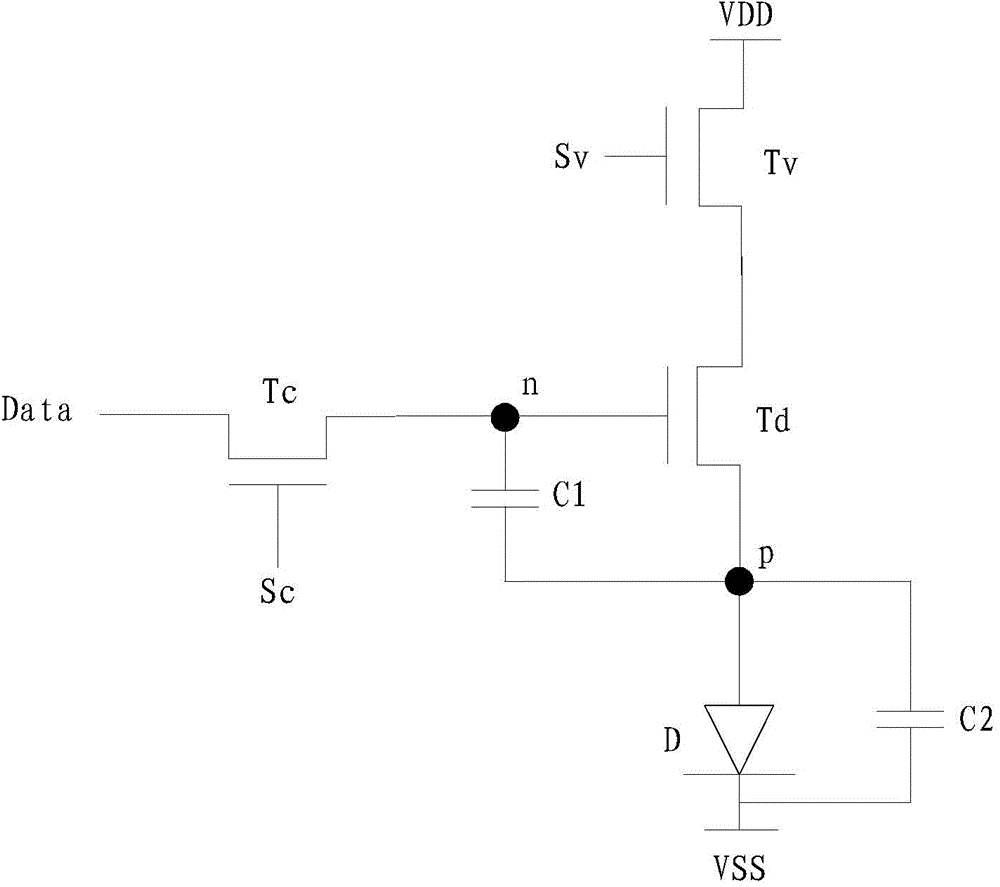
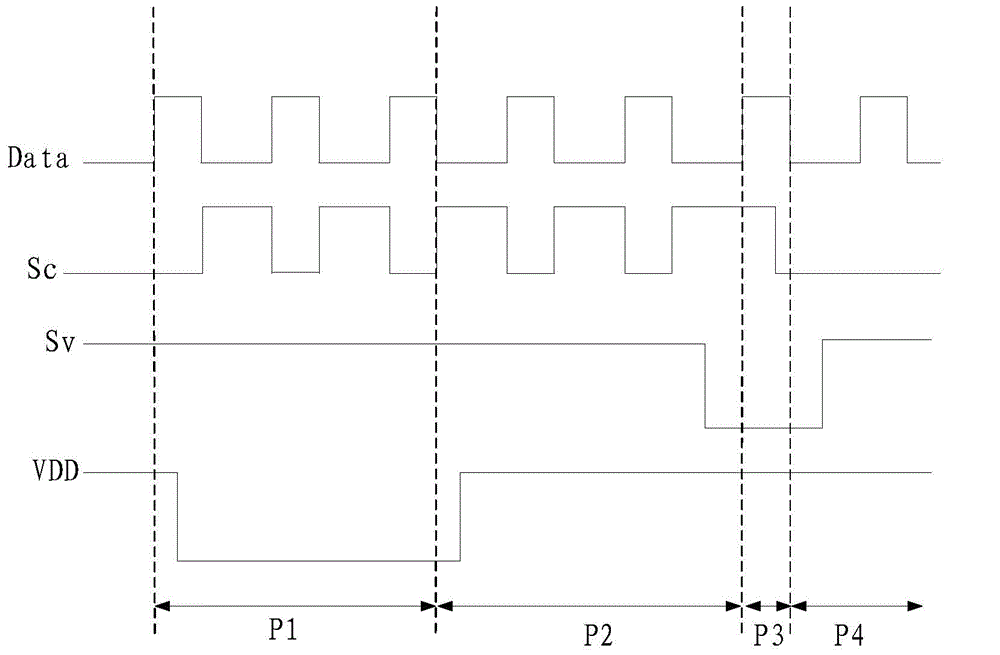
[0038] As mentioned in the background technology, the existing pixel driving circuit has high power consumption and complicated driving method. After a lot of experiments and research, the inventors of the present application found that one of the reasons for the aforementioned problems is: figure 2 As shown, it is a control timing diagram of an existing pixel driving circuit, and one frame (ie, one driving cycle) includes a reset period P1, a compensation period P2, a signal writing period P3 and a light emitting period P4.
[0039] In the reset period P1, when the gate control signal Sc is at a high potential, the control switch Tc is turned on, and at the same time, the data signal Data is at the reference potential Vref( figure 2 The low potential of the data signal Data is the reference potential Vref), so that the potential Vn=Vref of the input node n drives the gate-source voltage Vgs of the switching tube Td=Vn-Vp=Vref-Vp>Vth (wherein Vp is the voltage of the output n...
PUM
 Abstract
Description
Claims
Application Information
 - R&D
- Intellectual Property
- Life Sciences
- Materials
- Tech Scout
- Unparalleled Data Quality
- Higher Quality Content
- 60% Fewer Hallucinations
Browse by: Latest US Patents, China's latest patents, Technical Efficacy Thesaurus, Application Domain, Technology Topic, Popular Technical Reports.
© 2025 PatSnap. All rights reserved.Legal|Privacy policy|Modern Slavery Act Transparency Statement|Sitemap|About US| Contact US: help@patsnap.com


