Organic light emitting display device and method of manufacturing the same

A light-emitting display, organic technology, applied in the manufacture of semiconductor/solid-state devices, electrical components, diodes, etc., can solve the problems of light loss and reduce the brightness of OLED devices in the light transmittance of the display area.

Active Publication Date: 2015-05-20
LG DISPLAY CO LTD
View PDF5 Cites 14 Cited by
  • Summary
  • Abstract
  • Description
  • Claims
  • Application Information

AI Technical Summary

Problems solved by technology

[0016] However, in the OLED device according to the related art, the anti-reflection layer 90 generally provided in a film type is formed in both the TET region and the display region, which reduces the light transmittance of the display region and the brightness of the OLED device.
That is, in the case where light emitted from the light emitting layer 70 passes through the substrate 10 and then passes through the antireflection layer 90, a considerable amount of light is absorbed in the antireflection layer 90, thereby causing light loss.

Method used


Image

  • Organic light emitting display device and method of manufacturing the same
  • Organic light emitting display device and method of manufacturing the same
  • Organic light emitting display device and method of manufacturing the same

Examples


Embodiment Construction

[0035] Reference will now be made in detail to the preferred embodiments of the present invention, examples of which are illustrated in the accompanying drawings. Wherever possible, the same reference numbers will be used throughout the drawings to refer to the same or like parts.

[0036] In the following description, where a first element is positioned "on" or "over" a second element, the first element and the second element may be in contact with each other, or between the first element and the second element One or more third elements may be intervened. In addition, in case expressions such as “first” or “second” are used to refer to elements, the above terms may be used to distinguish any one element from other elements, but do not necessarily limit the order of the corresponding elements.

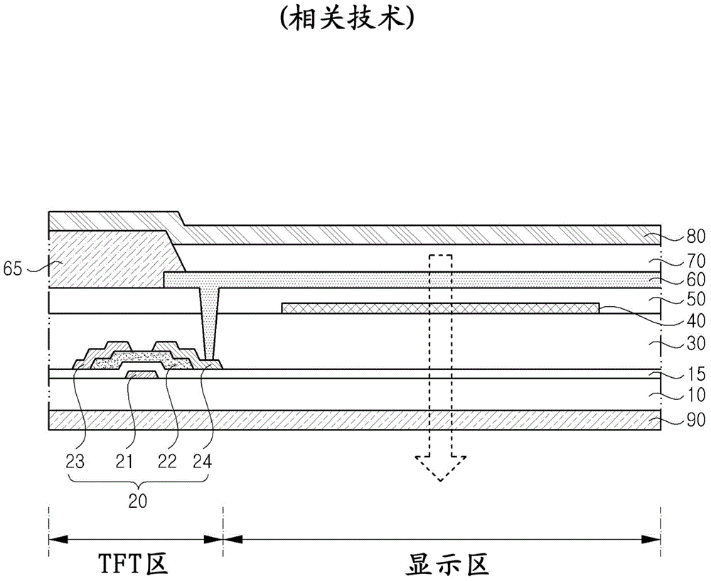
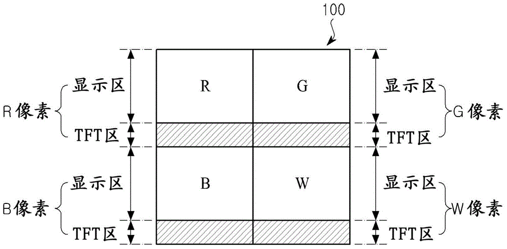
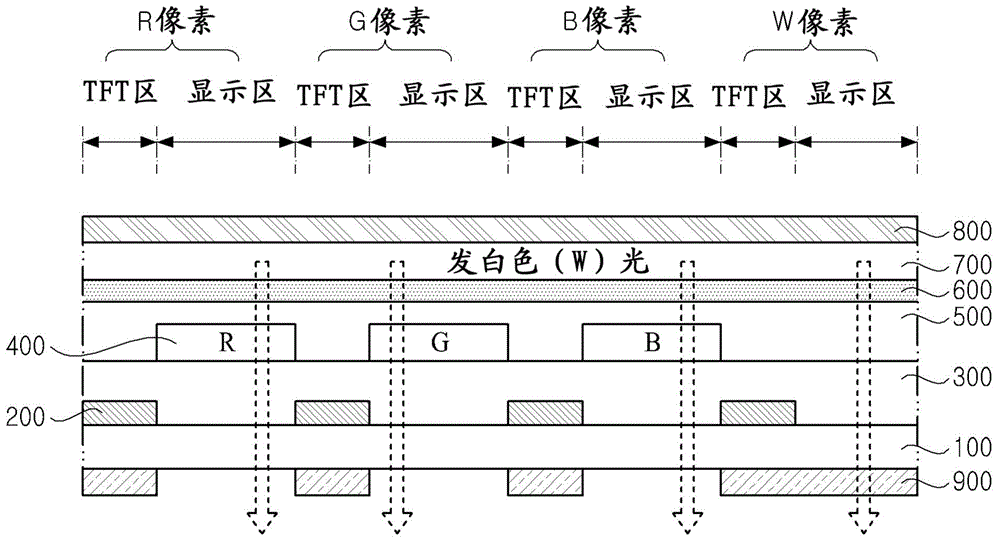
[0037] Hereinafter, an organic light emitting display (OLED) device and a method of manufacturing the same according to an embodiment of the present invention will be described in de...


PUM


Abstract

Disclosed is an organic light emitting display (OLED) device that may include first and second pixels on a substrate (100), each including a TFT region and a display region, the display region of each of the first and second pixels including a first electrode (600), an emission layer (700) and a second electrode (800); a color filter layer (400) in the display region of the second pixel; and a reflection preventing layer (900) in the first and second pixels, substantially excluding the display region of the second pixel.

Description

[0001] This application claims the benefit of Korean Patent Application No. 10-2013-0136465 filed on November 11, 2013, which is hereby incorporated by reference as if fully set forth herein. technical field [0002] The present invention relates to an organic light emitting display (OLED) device and a manufacturing method thereof, and more particularly to an OLED device provided with an anti-reflection layer and a manufacturing method thereof. Background technique [0003] An organic light emitting display (OLED) device includes a light emitting layer disposed between a negative electrode for injecting electrons and a positive electrode for injecting holes. When electrons generated in the negative electrode and holes generated in the positive electrode are injected into the inside of the light emitting layer, excitons are generated by recombination of the electrons and holes. Then, when the excitons drop from the excited state to a lower energy state, the OLED device emits ...

Claims


Application Information

Patent Timeline
IPC IPC(8): H01L27/32H01L51/56
CPCH10K59/351H10K59/38H10K59/12H10K50/86H10K50/84H10K50/85H10K50/868H10K59/122H10K59/1213H10K71/00
Inventor 朴沅基朴慧晶
Owner LG DISPLAY CO LTD
Why Eureka
Try Eureka