Multi-grid transistor and preparation method thereof

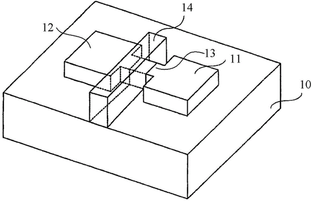
A transistor and multi-gate technology, applied in the field of multi-gate transistors and their preparation, can solve the problems of easy occurrence of abnormality, poor stability, damage of fins 13, etc., and achieve the effect of improving the reaction speed and avoiding easy damage.

Active Publication Date: 2015-04-29
SEMICON MFG INT (SHANGHAI) CORP
View PDF4 Cites 2 Cited by
  • Summary
  • Abstract
  • Description
  • Claims
  • Application Information

AI Technical Summary

Problems solved by technology

For example, under normal circumstances, the fins 13 are very thin, which easily leads to poor stability in the production process, and is prone to abnormalities when subjected to external influences.
For example, vibration and other situations will cause damage to the fins 13. Therefore, how to improve this problem is extremely important.

Method used


Image

  • Multi-grid transistor and preparation method thereof
  • Multi-grid transistor and preparation method thereof
  • Multi-grid transistor and preparation method thereof

Examples


preparation example Construction

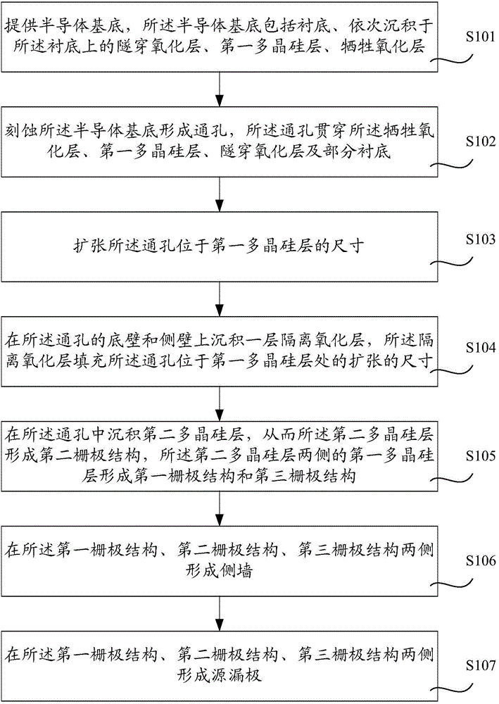
[0048] In combination with the above core ideas, the method for preparing a multi-gate transistor provided by the present invention includes:

[0049] Step S101, providing a semiconductor substrate, the semiconductor substrate comprising a substrate, a gate oxide layer deposited on the substrate in sequence, a first polysilicon layer, and a sacrificial oxide layer;

[0050] Step S102, etching the semiconductor substrate to form a through hole, the through hole passing through the sacrificial oxide layer, the first polysilicon layer, the gate oxide layer and part of the substrate;

[0051] Step S103, expanding the size of the through hole located in the first polysilicon layer;

[0052] Step S104, depositing an isolation oxide layer on the bottom wall and the side wall of the through hole, the isolation oxide layer filling the expanded size of the through hole at the first polysilicon layer;

[0053] Step S105, depositing a second polysilicon layer in the through hole, so that...


PUM

PropertyMeasurementUnit
heightaaaaaaaaaa
thicknessaaaaaaaaaa
thicknessaaaaaaaaaa

Abstract

The invention discloses a multi-grid transistor and a preparation method thereof. The preparation method comprises the following steps: providing a semiconductor substrate, wherein the semiconductor substrate comprises a substrate, a grid oxidation layer, a first polycrystalline silicon layer and a sacrificial oxidation layer; etching the semiconductor substrate to form a through hole; enlarging the size of the through hole formed in the first polycrystalline silicon layer; depositing an isolation oxidation layer on the bottom wall and the side wall of the through hole, wherein the isolation oxidation layer is filled in an enlarged part, which is positioned at the first polycrystalline silicon layer, of the through hole; depositing a second polycrystalline silicon layer in the through hole, so that the second polycrystalline silicon layer forms a second grid structure, and the first polycrystalline silicon layers at two sides of the second polycrystalline silicon layer form a first grid structure and a third grid structure; forming a side wall, a source electrode and a drain electrode at two sides of each of the first grid structure, the second grid structure and the third grid structure. According to the multi-grid transistor, the probability of damaging a fin type structure is avoided, the number of trenches is increased, and the speed of a device is increased.

Description

technical field [0001] The invention relates to the technical field of semiconductors, in particular to a multi-gate transistor and a preparation method thereof. Background technique [0002] In the advanced complementary metal oxide semiconductor (CMOS) industry, with the advent of 22nm and smaller dimensions, in order to improve the short channel effect and improve the performance of the device, the Fin Field-effect transistor (Fin Field-effect transistor, FinFET) is formed by Its unique structure is widely used. [0003] FinFET is a metal oxide semiconductor field effect transistor. Its structure is usually formed on a silicon-on-insulator substrate, including narrow and independent silicon strips, as a vertical channel structure, also known as fins, on both sides of the fins There is a gate structure. In general, FinFETs have smaller device structures and better performance. [0004] Such as figure 1 As shown, it is a schematic structural diagram of a FinFET in the p...

Claims


Application Information

Patent Timeline
Patent Type & Authority Applications(China)
IPC IPC(8): H01L21/331H01L29/10H01L29/739
CPCH01L29/4232H01L29/66484H01L29/7831
Inventor 赵猛
Owner SEMICON MFG INT (SHANGHAI) CORP
Why Eureka
Try Eureka