A pcb design layout checking device

A layout and audit point technology, applied in the field of PCB design layout audit device, can solve problems such as difficult interactive positioning of pcb design system, long audit cycle, cumbersome data preparation, etc., to reduce research and development costs, shorten research and development cycle, and improve audit operations sexual effect

Active Publication Date: 2020-04-07
SHANGHAI TAIQI ELECTRONICS TECH CONSULTATIONCO
View PDF3 Cites 0 Cited by
  • Summary
  • Abstract
  • Description
  • Claims
  • Application Information

AI Technical Summary

Problems solved by technology

[0003] The above review tools have the following disadvantages: the data preparation before the review is cumbersome, and the results after the review are not easy to interact with the pcb design system
For the problems found in the audit, after the pcb design system is changed, it is necessary to output odb++ data or gerber data for re-audit confirmation, so many repetitions, the audit cycle is very long

Method used


Image

  • A pcb design layout checking device
  • A pcb design layout checking device
  • A pcb design layout checking device

Examples


Embodiment Construction

[0025] In order to make the object, technical solution and advantages of the present invention clearer, the present invention will be further described in detail below in combination with specific examples and with reference to the accompanying drawings. It should be understood that these descriptions are exemplary only, and are not intended to limit the scope of the present invention. Also, in the following description, descriptions of well-known structures and techniques are omitted to avoid unnecessarily obscuring the concept of the present invention.

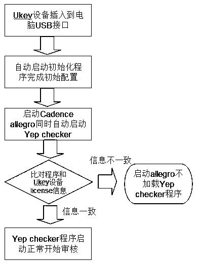
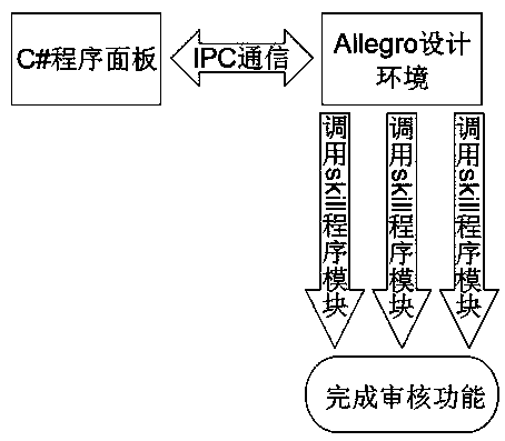
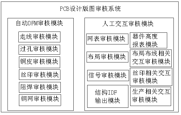
[0026] Such as figure 1 or figure 2 As shown: a PCB design layout review device of the present invention, including a device memory, the device memory is provided with an automatic DFM review module and a manual interactive review module; the automatic DFM review module includes a wiring review module and a via hole review module , a copper skin audit module, a silk screen audit module, a solder mask audit module and a st...


PUM


Abstract

The invention discloses a PCB design layout audit device, the PCB design layout audit device comprises a device storage, the device storage is provided with the an automatic DFM audit module and a man-machine interaction audit module; the automatic DFM audit module comprises a line audit module, a via hole audit module, a copper sheet audit module, a silk screen audit module, a solder resist audit module and a steel mesh audit module; the man-machine interaction audit module comprises a netlist audit module, a layout audit module, a signal audit module, a structure IDF output module, a device height reporting module, a locating and wiring related interaction audit module, a silk screen related interaction audit module and a production related interaction audit module. The audit system is independently prepared into the electronic product device to be conveniently used by the customers in a plug and play mode, and the audit system is not limited by the mounting computer anymore. The Ukey device is inserted into the computer for the corresponding engineer and the PCB design audit can be executed according to the requirement from the engineer.

Description

technical field [0001] The invention belongs to the field of printed circuit board design in electronic product development technology, and in particular relates to a PCB design layout checking device. Background technique [0002] At home and abroad, there are pcb design layout DFM review tools, which are used to automatically review the final results of pcb design by importing odb++ data or gerber data third-party data output by the pcb design system. [0003] The above review tools have the following disadvantages: the data preparation before review is cumbersome, and the results after review are not easy to interact with the pcb design system for positioning. For the problems found in the review, after the pcb design system is changed, it is necessary to output the odb++ data or gerber data for re-review and confirmation. With so many repetitions, the review cycle is very long. Contents of the invention [0004] In order to solve the above-mentioned problems existing ...

Claims


Application Information

Patent Timeline
Patent Type & Authority Patents(China)
IPC IPC(8): G06F30/392G06F119/18
Inventor 叶恩齐
Owner SHANGHAI TAIQI ELECTRONICS TECH CONSULTATIONCO
Why Eureka
Try Eureka