Lead-less ball foot surface adhesion type microwave film hybrid integrated circuit and integration method thereof

A hybrid integrated circuit, microwave thin film technology, applied in the direction of circuits, electrical components, electric solid devices, etc. There are many leads, etc., to achieve broad market prospects and application space, reduce the volume, and improve the effect of high-frequency performance

Inactive Publication Date: 2015-04-01
GUIZHOU ZHENHUA FENGGUANG SEMICON
View PDF3 Cites 9 Cited by
  • Summary
  • Abstract
  • Description
  • Claims
  • Application Information

AI Technical Summary

Benefits of technology

This patented technology describes an electronic component called this type of chip (C) mounted on a small area of plastic or rubber material. These C' s are designed without any external packages like solder connections between components. They have several technical benefits such as reducing size, eliminating extra parts, higher density, better signal quality, enhancing durability, being able to integrate multiple function modules within one unit, increasing functionality while maintaining compactness, and providing protection against damage from environmental factors during operation. Overall, these improvements make them more efficient than existing devices due to their smaller sizes and lesser number of necessary features compared to traditional methods.

Problems solved by technology

Technological Problem addressed by this patented technical problem relates to reducing package size while maintaining good performance at very small sizes due to the limitations associated with traditional methods like welding metal lines between electronic devices and solder connections that can cause signal distortion during operation.

Method used


Image

  • Lead-less ball foot surface adhesion type microwave film hybrid integrated circuit and integration method thereof
  • Lead-less ball foot surface adhesion type microwave film hybrid integrated circuit and integration method thereof
  • Lead-less ball foot surface adhesion type microwave film hybrid integrated circuit and integration method thereof

Examples


Embodiment Construction

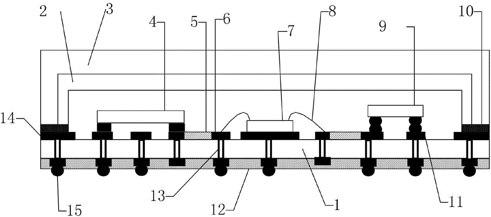
[0032] structured as figure 1 The non-lead ball surface-mounted microwave thin film hybrid integrated circuit is composed of a thin film ceramic substrate 1, a thin film conduction band, a thin film stop band 5, a thin film capacitor, a thin film inductor, a chip component 4, a semiconductor bare chip and a cap; There is a metallized through hole between the front and bottom of the thin film ceramic substrate; the thin film conduction band, the thin film stop band 5, the thin film capacitor and the thin film inductor are integrated on the front of the thin film ceramic substrate 1, and an insulating medium is used on the bottom surface of the thin film ceramic substrate 1 The film 12 is sealed and insulated and protected; the metal ball-type external connection end is made on the bottom surface of the film ceramic substrate 1; Capacitor, thin film inductor, semiconductor bare chip; Semiconductor bare chip comprises front-mounted semiconductor chip 7 and flip-chip semiconductor...


PUM


Abstract

The invention discloses a lead-less ball foot surface adhesion type microwave film hybrid integrated circuit and an integration method thereof. The integrated circuit consists of a film ceramic substrate, film conduction bands, film stop bands, a film capacitor, a film inductor, chip components, semiconductor naked chips and a tube cape, wherein through holes are formed between the front side and the bottom side of the film ceramic substrate; the film conduction bands, the film stop bands, the film capacitor and the film inductors are integrated on the front side of the film ceramic substrate; the bottom side of the film ceramic substrate is protected by using an insulating medium film; the bottom side of the film ceramic substrate is a ball foot type external connecting end; the tube cap is mounted on the front side of the film ceramic substrate in an adhesion manner; positively mounted semiconductor naked chips are connected with the film stop bands through bonding wires; inversely mounted semiconductor naked chips are welded with metal ball feet through ball feet; a metal layer is arranged on the outer layer of the tube cap; a ceramic coating layer is arranged on the inner wall of the tube cap. The integration method comprises the following steps: preparing materials, forming holes, washing, forming a graphic network, welding, assembling, bonding, capping, and the like. A device adopting the lead-less ball foot surface adhesion type microwave film hybrid integrated circuit is wide in application and is particularly applicable to the field of small-size facility systems.

Description


Claims


Application Information

Patent Timeline
Owner GUIZHOU ZHENHUA FENGGUANG SEMICON
Why Eureka
Try Eureka