
Patsnap Eureka
For R&D, Patsnap Eureka makes reading and utilizing patents & technical documents easy.
Patsnap Eureka AIR
Designed for self-driven R&D workflows. Generate viable solutions, solve complex R&D challenges, empower your innovation with AI.

Patsnap Eureka Materials
Designed for material experts only. Revolutionize your material R&D, from search, analyze, to developing new materials.

TechResearch
Generate reliable direction feasibility study reports for your R&D in just a few steps.

TechSeek
Discover and master advanced knowledge NOW. Basics, ideas, possibilities, all at once.

TechMind
As an expert in R&D Theories, TechMind can generates customized viable solutions instantly.

TechRisk
Analyze your overall solution with one click, know your potential R&D risks in advance.

TechMonitor
Get weekly tech updates, stay abreast of the latest tech innovations and key insights.
Method for manufacturing photomask, method for manufacturing display device, and drawing device
一种制造方法、显示装置的技术,应用在光掩模领域,能够解决工作台不充分平坦性、基板挠曲、膜面形状一致等问题
- Summary
- Abstract
- Description
- Claims
- Application Information
AI Technical Summary
Problems solved by technology
Method used
Image


Examples
Embodiment approach 1
[0116] The manufacturing method of the photomask of this invention has the following process.
[0117] Preparation of Photomask Blanks
[0118] In the present invention, drawing for forming a photomask based on a pattern designed based on a desired device is performed on a photomask blank formed on a main surface of a substrate. One or more thin films, and photoresist films are obtained. Therefore, a photomask blank in which the above-mentioned thin film and photoresist film were formed on one main surface of the substrate was prepared.
[0119] As the photomask blank to be prepared, a known photomask blank can be used.
[0120] As the substrate, a transparent substrate such as quartz glass can be used. Although the size and thickness are not limited, as the substrate used in the manufacture of a device for a display device, a substrate having a side of 300 mm to 1800 mm and a thickness of about 5 to 15 mm can be used.
[0121] In this application, in addition to the subst...
Embodiment approach 2
[0257]
[0258] As described above, according to the present invention, it is possible to obtain a photomask capable of extremely high coordinate accuracy of a pattern formed on a workpiece.
[0259] In addition, when such a photomask is inspected before shipment, it is most desirable to inspect in consideration of the difference between the photomask placed on the inspection device and the photomask held on the exposure device.
[0260] Therefore, the inventors found the necessity of a new inspection method.
[0261] VII Process of Obtaining Pattern Coordinate Data L
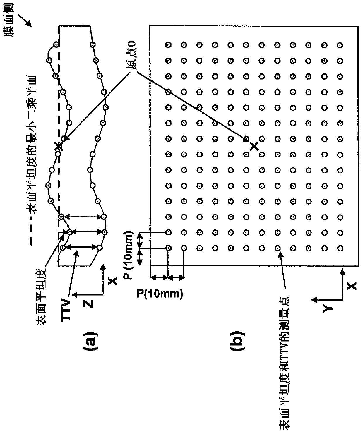
[0262] The patterned photomask was placed on the table of the coordinate inspection apparatus so that the film surface (pattern formation surface) was on the upper side, and coordinate measurement was performed. The data obtained here are assumed to be pattern coordinate data L.
[0263] Here, it is preferable to perform coordinate measurement by measuring the coordinates of the mark pattern previously form...
Embodiment
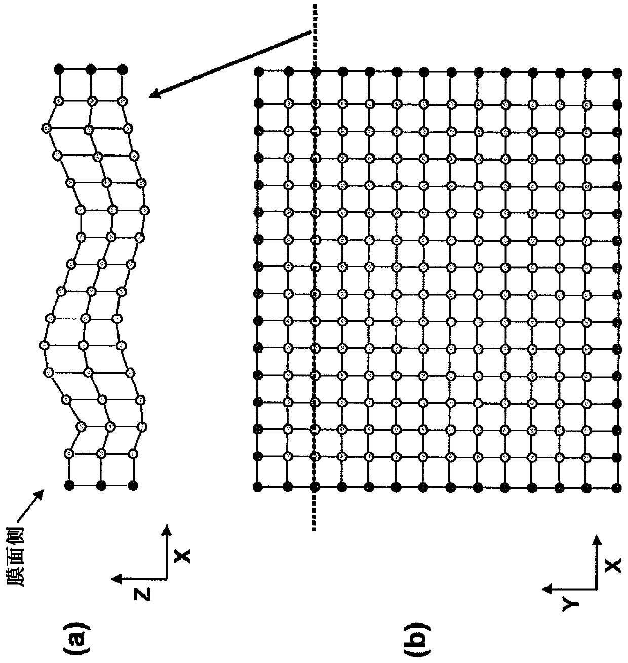
[0304] use Figure 12 The schematic diagram shown shows the effect of the invention based on the photomask manufacturing method (drawing process) of the present invention.
[0305] Here, the result obtained by simulation is shown in the case where a pattern for transfer is drawn on a substrate (photomask blank) having a specific substrate surface shape (substrate surface shape data B), where How does the coordinate accuracy of the transfer pattern change when it reaches the inside of the exposure device (as a result, how does the coordinate accuracy of the pattern formed on the transfer target change).
[0306]First, a specific test pattern was drawn on the above-mentioned photomask blank using a drawing device. In the test photomask blank used here, a light-shielding film and a positive photoresist film were formed on the main surface of a quartz substrate having a size of 800 mm×920 mm.
[0307] As the pattern design data used here, a test pattern including a cross pattern...
PUM
| Property | Measurement | Unit |
|---|---|---|
| density | aaaaa | aaaaa |
Abstract
Description
Claims
Application Information
 - R&D Engineer
- R&D Manager
- IP Professional
- Industry Leading Data Capabilities
- Powerful AI technology
- Patent DNA Extraction
Browse by: Latest US Patents, China's latest patents, Technical Efficacy Thesaurus, Application Domain, Technology Topic, Popular Technical Reports.
© 2024 PatSnap. All rights reserved.Legal|Privacy policy|Modern Slavery Act Transparency Statement|Sitemap|About US| Contact US: help@patsnap.com