
Device and method for transferring CVD grown graphene

A transfer method and transfer device technology, applied in the field of thin film materials, can solve problems such as cracking, sample performance impact, residue and so on

Inactive Publication Date: 2015-02-25
JIANGNAN GRAPHENE RES INST +1
View PDF5 Cites 11 Cited by
  • Summary
  • Abstract
  • Description
  • Claims
  • Application Information

AI Technical Summary

Problems solved by technology

Although it has been reported that 30-inch graphene samples can be grown in terms of preparation, there is still a long way to go for practical application, because most of the sample quality degradation phenomena (such as wrinkles, cracks, etc.) still occur in the graphene transfer process. in process
The current transfer process can be mainly divided into dry transfer and wet transfer. Among them, roll-to-roll is a typical dry transfer, but it limits the target substrate to be a flexible substrate. For Si wafer, Al 2 o 3 Equal rigid substrates are not applicable; the current wet transfer method requires the help of organic substances (such as PDMS, PMMA), although they better maintain the intrinsic morphology of graphene during the transfer process, but it is difficult to be completely removed after the transfer is completed. Remove, remain on the sample, and affect the performance of the sample

Method used


Image

  • Device and method for transferring CVD grown graphene
  • Device and method for transferring CVD grown graphene
  • Device and method for transferring CVD grown graphene

Examples


Embodiment 1

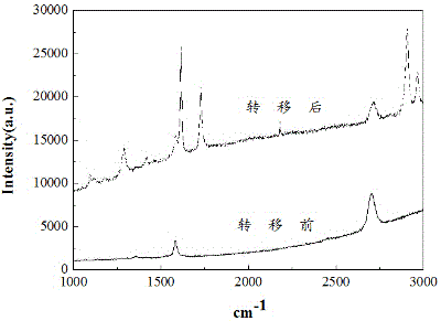
[0026] 1) Graphene was grown on the Cu substrate by chemical vapor deposition, and the graphene grown on the back of the substrate was removed by oxygen plasma; 2) PET was fixed at the same end as the single-sided graphene / Cu sample obtained in step 1) On the wall of the container with a circular hole with a diameter of 10 mm hollowed out at the bottom, the PET is parallel to the liquid surface of the ferric chloride solution, and the single-sided graphene / Cu sample is inserted below the liquid surface at 30 degrees; 3) Step 2) Immersed in the liquid The Cu part under the surface is etched first, adjust the position of the liquid level of the hollow container, so that the graphene and PET are in contact with each other, that is, the transfer is completed first; 4) Use a syringe to adjust the position of the liquid level of the ferric chloride solution, and repeat step 3) Etching and transfer operations, so that the single-sided graphene sample is gradually etched from the free ...

Embodiment 2

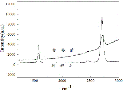
[0028] 1) Graphene was grown on the Cu substrate by chemical vapor deposition, and the graphene grown on the back of the substrate was removed by oxygen plasma cleaning; 2) Si was placed at the same end as the single-sided graphene / Cu sample obtained in step 1) Fixed on the wall of a hexagonal container with a hollow bottom diameter of 10 mm, where Si is parallel to the liquid surface of the ammonium persulfate solution, and the single-sided graphene / Cu sample is inserted below the liquid surface at 20 degrees; 3) Step 2) Immersed in The Cu part under the liquid surface is first etched, adjust the liquid surface position of the hollow container, make the graphene and Si contact and bond, that is, the transfer is completed first; 4) Adjust the liquid surface position of the ammonium persulfate solution with a syringe, repeat step 3) Etching and transfer operations, so that the single-sided graphene sample is gradually etched from the free end to the fixed end until all the etchi...

example 3

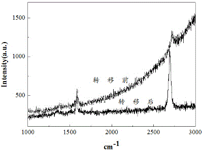
[0030] 1) Graphene was grown on the Cu substrate by chemical vapor deposition, and the graphene grown on the back of the substrate was removed by oxygen plasma cleaning; 2) Al 2 o 3 The same end of the single-sided graphene / Cu sample obtained in step 1) is fixed on the wall of a container with a hollow bottom and a side length of 10mm square, where Al 2 o 3 Parallel to the liquid surface of the potassium persulfate solution, the single-sided graphene / Cu sample is inserted below the liquid surface at 10 degrees; 3) The Cu part immersed in the liquid surface in step 2) is etched first, and the liquid surface position of the hollow container is adjusted, Make graphene and Al 2 o 3 Contact and fit, that is, the transfer is completed first; 4) Use a syringe to adjust the liquid level of the potassium persulfate solution, repeat the etching and transfer in step 3), so that the single-sided graphene sample is gradually etched from the free end to the fixed end until All etching i...


PUM

PropertyMeasurementUnit
surface areaaaaaaaaaaa

Abstract

The invention relates to a device and a method for transferring CVD grown graphene. The method comprises the specific steps: 1) removing the graphene grown on the back of a corresponding substrate by use of a chemical vapor deposition method; 2) fixing the same ends of a target substrate and a growth substrate / single-sided graphene sample obtained in the step 1) on the wall of a bottom hollowed-out container, wherein the target substrate is parallel to the liquid level of an etchant, while the growth substrate / single-sided graphene sample is inserted under the liquid level; 3) firstly etching the part, immersed under the liquid level, of the growth substrate, and adjusting the position of the liquid level in the hollowed-out container so that the graphene is in contact and fitted with the target substrate, thereby finishing transfer; 4) continuing to adjust the position of the liquid level of the etchant, repeating the etching and transfer operations in the step 3) and gradually etching the single-sided graphene sample from a free end to a fixed end until all the etching is completed. According to the method for transferring the CVD grown graphene, the pollution problem of organic component residual due to organic matters such as PMMA used in the existing graphene transfer technology is avoided, the transfer process is simplified, and a novel process of transferring a continuous large-area and high-quality graphene sample while etching is realized.

Description

technical field [0001] The invention relates to a method for transferring graphene, which belongs to the field of thin film materials. Background technique [0002] Graphene is a carbon atom in a two-dimensional plane with SP 2 Hexagonal structure formed by orbital hybridization. Due to the π bond in the structure, graphene exhibits excellent thermal, electromagnetic and mechanical properties (according to literature reports thermal conductivity 5000Wm -1 K -1 , the intrinsic mobility reaches 200,000 cm 2 v -1 the s -1 , the optical transmittance is 97.7%, and the surface area reaches 2630 m 2 g -1 , Young's modulus 1.0TPa,). Therefore, graphene has not only become a "star material" in the minds of many scientific researchers, but also attracts more and more entrepreneurs to push it to industrialization. In the process of graphene moving towards practical application, there are two main obstacles: preparation and transfer. Although it has been reported that 30-in...

Claims


Application Information

Patent Timeline
Patent Type & Authority Applications(China)
IPC IPC(8): C01B31/04
Inventor 贾宝平王小周丁建宁
Owner JIANGNAN GRAPHENE RES INST
Learn More