A single bus receive logic structure
A logical structure, single-bus technology, applied in the electronic field, can solve problems such as execution effect dependence, consumption of CPU resources, speed of receiving code rate, limited operating clock cycle, etc., to achieve less resource consumption, realization of reception, and fast processing speed Effect
- Summary
- Abstract
- Description
- Claims
- Application Information
AI Technical Summary
Problems solved by technology
Method used
Image
Examples
Embodiment Construction
[0015] The present invention will be further described in detail below in conjunction with the accompanying drawings and specific embodiments.
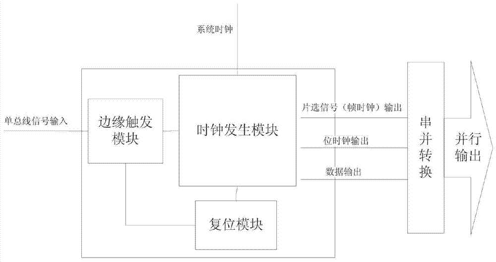
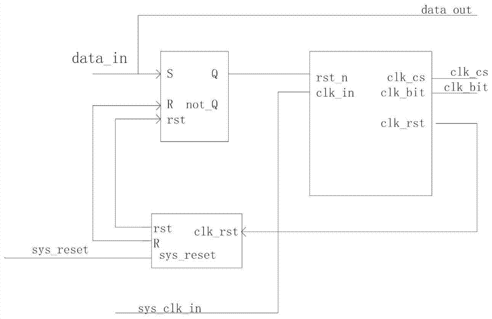
[0016] Such as figure 1 The schematic diagram of the bus receiving logic structure shown includes an edge trigger module, a clock generation module and a reset module, where the edge trigger module is connected to the clock generation module and the reset module respectively, the clock generation module is connected to the reset module, and the clock generation module is connected to the system The clock is connected, and the edge trigger module is connected to the single bus signal input terminal, which is used to identify the starting edge of the data code string and enable the clock generator to start clock counting. The reset module provides a global reset signal and controls the When the output signal is enabled, the receiving end receives the frame reset signal; the clock generation module starts counting after the edge trigger ...
PUM
 Abstract
Description
Claims
Application Information
 - R&D
- Intellectual Property
- Life Sciences
- Materials
- Tech Scout
- Unparalleled Data Quality
- Higher Quality Content
- 60% Fewer Hallucinations
Browse by: Latest US Patents, China's latest patents, Technical Efficacy Thesaurus, Application Domain, Technology Topic, Popular Technical Reports.
© 2025 PatSnap. All rights reserved.Legal|Privacy policy|Modern Slavery Act Transparency Statement|Sitemap|About US| Contact US: help@patsnap.com


