Device and method for protecting graphene film in etching and transfer
A graphene film and transfer device technology, which is applied in the manufacture of graphene, electrical components, semiconductors/solid devices, etc., can solve the problems of graphene sheet damage, graphene damage, and residual bubbles on the catalytic substrate, so as to achieve convenient transfer, The effect of avoiding damage
- Summary
- Abstract
- Description
- Claims
- Application Information
AI Technical Summary
Problems solved by technology
Method used
Image
Examples
Embodiment 1
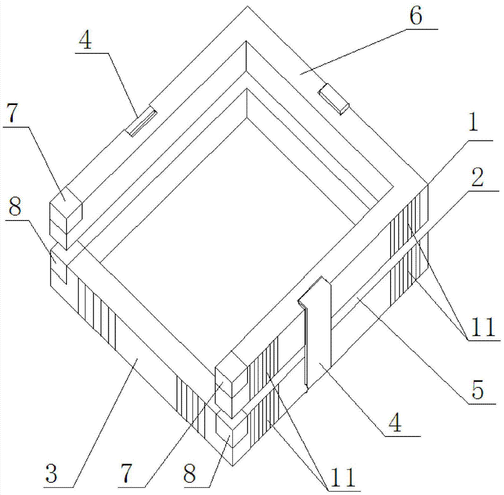
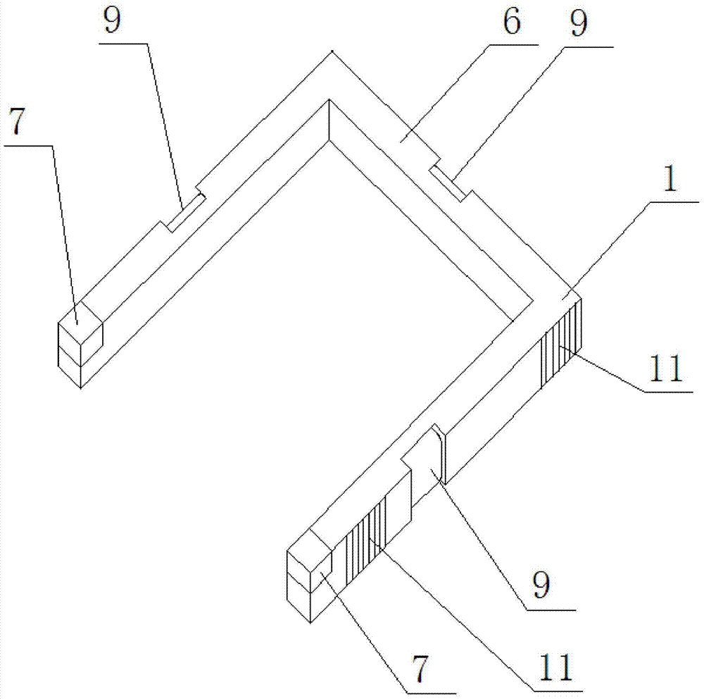
[0044]This embodiment includes a first clamp 1 and a second clamp 2, the first clamp 1 is a square frame structure composed of first clamp columns 6, and the second clamp 2 is composed of four second clamp columns 3 Square frame structure, the square size of the first clamp 1 is the same as the square size of the second clamp 2, and the first clamp 1 is arranged above the second clamp 2, the first clamp 1 and The second clamp 2 is connected by a movable buckle 4, and a clamp gap 5 is provided between the first clamp 1 and the second clamp 2, such as figure 1 shown. Such as image 3 , Figure 5 The first fixture 1 shown is a square frame structure with an open side on one side consisting of three first fixture columns 6, and the first fixture 1 is provided with a frame for identifying the first fixture 1 and sensing the first fixture 1. A first clamp sensing chip 7 for the position of the first clamp 1 , and a second clamp sensing chip 8 for identifying the second clamp 2 an...
Embodiment 2
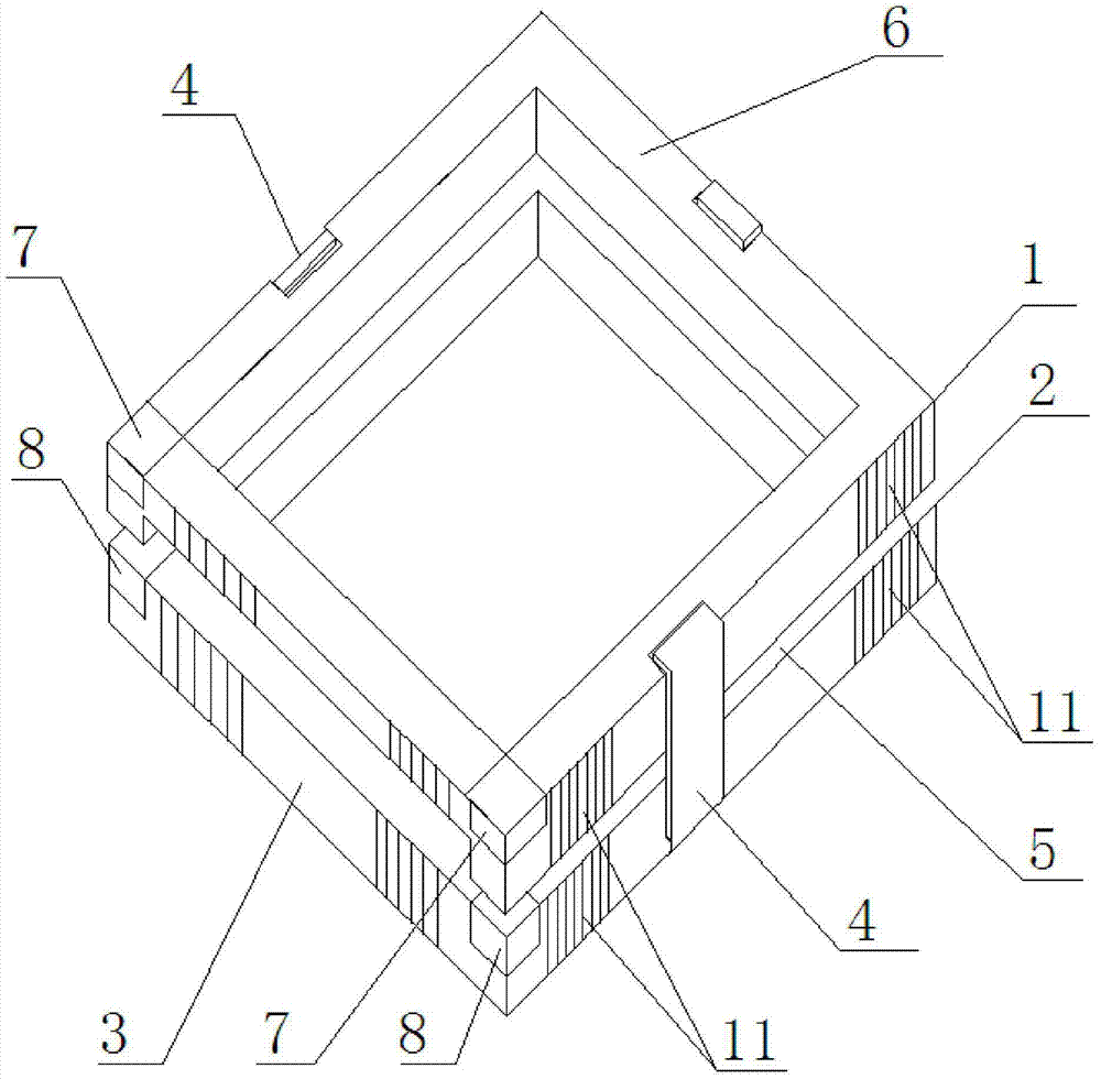
[0053] This embodiment includes a first clamp 1 and a second clamp 2, the first clamp 1 is a square frame structure, the second clamp 2 is a square frame structure composed of four second clamp columns 3, the first The square size of the clamp 1 is the same as the square size of the second clamp 2, the first clamp 1 and the second clamp 2 are connected by a movable buckle 4, the first clamp 1 and the second clamp 2 between fixture gaps 5, such as figure 2 shown. Such as Figure 4 , Figure 5 As shown, the first clamp 1 is a square frame structure consisting of four first clamp columns 6 with the lower surface in the same plane, one of the four first clamp columns 6 forming the first clamp 1 The thickness of the first clamp column 6 is smaller than the other three first clamp columns 6, and the first clamp 1 is provided with a first device for identifying the first clamp 1 and sensing the position of the first clamp 1. Clamp sensing chip 7, the second clamp sensing chip 8 ...
PUM
 Abstract
Description
Claims
Application Information
 - R&D Engineer
- R&D Manager
- IP Professional
- Industry Leading Data Capabilities
- Powerful AI technology
- Patent DNA Extraction
Browse by: Latest US Patents, China's latest patents, Technical Efficacy Thesaurus, Application Domain, Technology Topic, Popular Technical Reports.
© 2024 PatSnap. All rights reserved.Legal|Privacy policy|Modern Slavery Act Transparency Statement|Sitemap|About US| Contact US: help@patsnap.com


