Chip plastic package structure manufacturing method

A manufacturing method and chip technology, applied in semiconductor/solid-state device manufacturing, semiconductor devices, electrical components, etc., can solve the problems of high manufacturing cost and low cost, and achieve the effect of low cost and simple process

Inactive Publication Date: 2014-12-24
INST OF MICROELECTRONICS CHINESE ACAD OF SCI +1
View PDF3 Cites 7 Cited by
  • Summary
  • Abstract
  • Description
  • Claims
  • Application Information

AI Technical Summary

Problems solved by technology

[0005] The embodiment of the present invention provides a method for manufacturing a chip plastic packaging structure, which is used to solve the technical problem of high manufacturing cost of the wire bonding plastic packaging structure and method in the prior art, and has a technical effect of low cost

Method used


Image

  • Chip plastic package structure manufacturing method
  • Chip plastic package structure manufacturing method
  • Chip plastic package structure manufacturing method

Examples


Embodiment 1

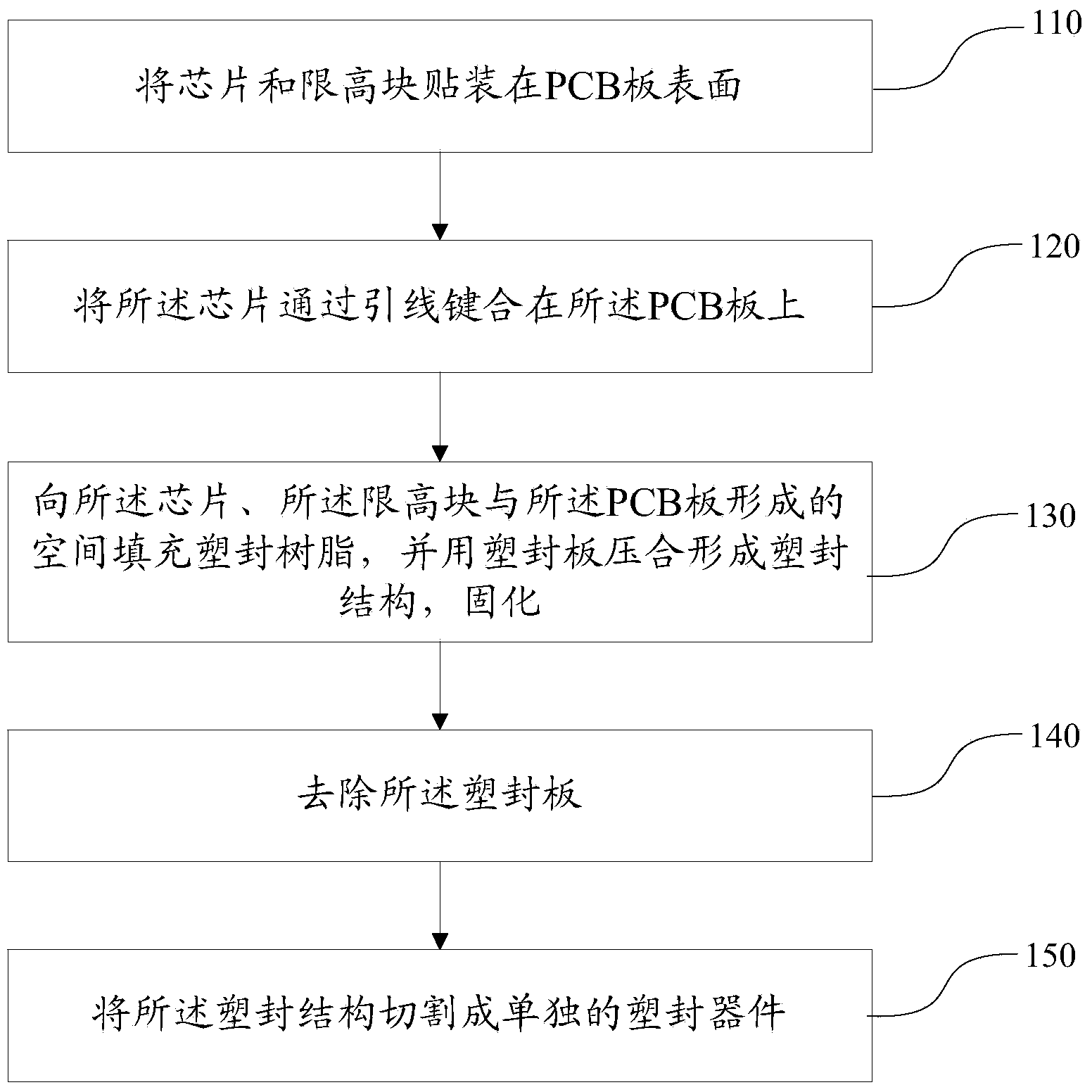
[0032] In order to enable those skilled in the art to understand the present invention in more detail, the present invention will be described in detail below in conjunction with the accompanying drawings.

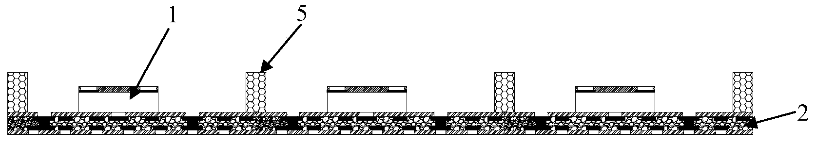
[0033] Such as Figure 2-6 As shown, the embodiment of the present invention also provides a method for manufacturing a chip plastic package structure, the method comprising:

[0034] Step 110: mount the chip 1 and the height limiting block 5 on the surface of the PCB board 2;

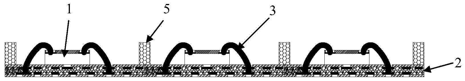
[0035] Step 120: bonding the chip 1 on the PCB 2 through the wire 3;

[0036] Step 130: Fill the space formed by the chip 1, the height limiting block 5 and the PCB board 2 with a plastic sealing resin 4, press the plastic sealing plate 6 to form a plastic sealing structure, and cure;

[0037] Step 140: removing the plastic sealing plate 6;

[0038] Step 150: Cut the molded structure into individual molded devices.

[0039] Further, filling the molding resin in step 130 also includes:

[0040]...


PUM


Abstract

The invention discloses a chip plastic package structure manufacturing method and relates to the technical field of semiconductors. The method includes the steps that a chip and height limiting blocks are attached to the surface of a PCB; the chip is arranged on the PCB in a bonding mode through a lead, the space formed by the chip, the height limiting blocks and the PCB is filled with plastic package resin, a plastic package structure is formed through press fit of a plastic package plate, and curing is performed; a plastic package plate is removed; the plastic package structure is cut to form independent plastic package devices. Due to the use of the height limiting blocks, a high-precision packaging mold is not needed, and the low-cost advantage is achieved.

Description

technical field [0001] The invention relates to the technical field of semiconductors, in particular to a method for manufacturing a chip plastic packaging structure. Background technique [0002] In the field of semiconductor technology, commonly used chips are bonded to the surface of the PCB, among which wire bonding is more commonly used. [0003] But, those skilled in the art find that there is following deficiency in the prior art through research: [0004] Although the conventional method in the prior art is simple and easy to mass produce, it needs to make high-precision molds, and different molds need to be made for different packaging heights. Due to the high cost of making molds, the manufacturing cost is high. Contents of the invention [0005] The embodiment of the present invention provides a method for manufacturing a chip plastic packaging structure, which is used to solve the technical problem of high manufacturing cost of the wire bonding plastic packagi...

Claims


Application Information

Patent Timeline
IPC IPC(8): H01L21/50H01L21/56
CPCH01L21/56H01L21/561H01L2224/48091H01L2224/48227H01L2224/73265H01L2224/92247H01L2224/97H01L2924/00014
Inventor 于中尧郭学平
Owner INST OF MICROELECTRONICS CHINESE ACAD OF SCI
Why Eureka
Try Eureka