
Display panel, and pixel structure and driving method for display panel

A pixel structure and pixel technology, applied in the direction of static indicators, nonlinear optics, instruments, etc., can solve the problems of three-dimensional display crosstalk, affect the penetration rate of two-dimensional display, and cannot achieve low color shift effect, etc., to achieve good low color Offset effect, ensure the penetration rate, improve the effect of image display quality

Inactive Publication Date: 2014-12-24
TCL CHINA STAR OPTOELECTRONICS TECH CO LTD
View PDF4 Cites 10 Cited by
  • Summary
  • Abstract
  • Description
  • Claims
  • Application Information

AI Technical Summary

Problems solved by technology

[0004] In order to avoid crosstalk in 3D display, liquid crystal display panel manufacturers will appropriately increase the shading distance between adjacent pixels in the upper and lower lines when designing the 3D FPR pixel structure, but this will affect the transmittance under 2D display conditions
At the same time, the liquid crystal display panel cannot achieve the above-mentioned low color shift effect under the condition of three-dimensional display

Method used


Image

  • Display panel, and pixel structure and driving method for display panel
  • Display panel, and pixel structure and driving method for display panel
  • Display panel, and pixel structure and driving method for display panel

Examples


Embodiment Construction

[0044] In order to make the purpose, technical solution and advantages of the present invention clearer, the present invention will be further described in detail below in conjunction with specific embodiments and accompanying drawings.

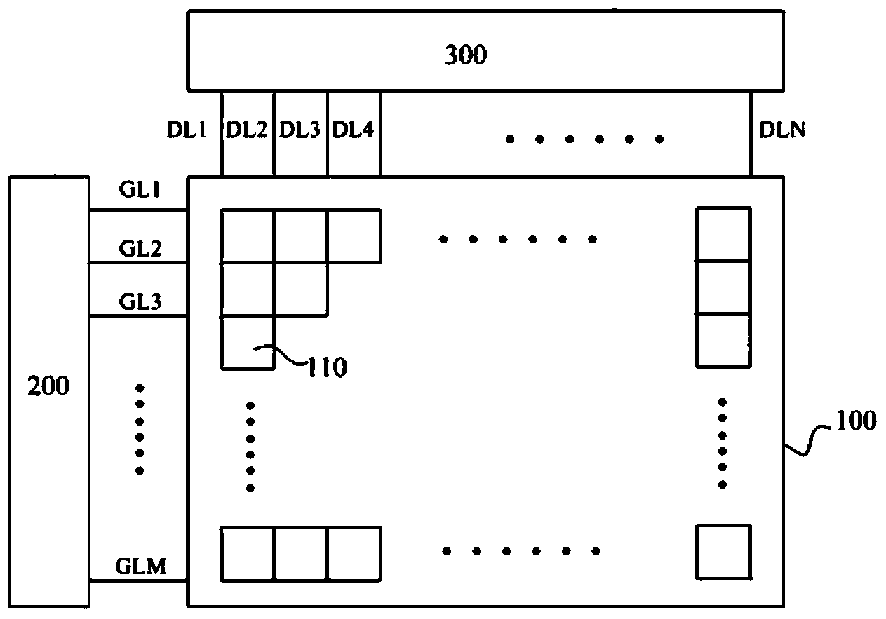
[0045] figure 1is a schematic structural diagram of a display panel drawn according to Embodiment 1 of the present invention. The display panel includes an image display area 100 , a scan driving circuit 200 and a data driving circuit 300 . The image display area 100 includes an array formed by a plurality of scan lines GL1 -GLM and a plurality of data lines DL1 -DLN arranged in a staggered manner, and a plurality of pixel structures 110 as elements of the array. Wherein, the scanning driving circuit 200 transmits the provided scanning signals to the pixel structures 110 in the image display area 100 through a plurality of scanning lines GL1 -GLM coupled thereto. The data driving circuit 200 transmits the provided data signals to the pixel ...


PUM


Abstract

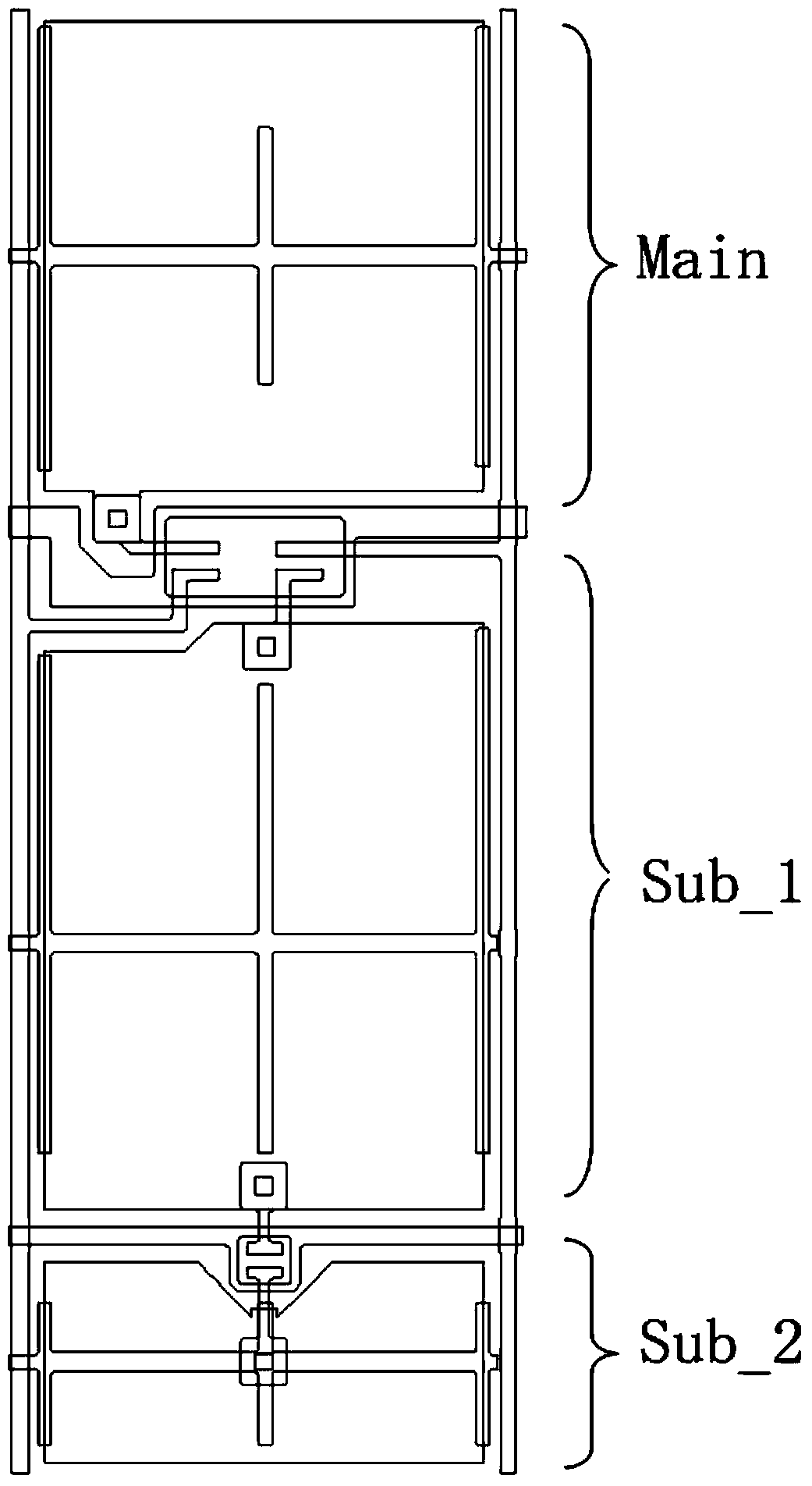
The invention discloses a display panel, and a pixel structure and a driving method for the display panel. The pixel structure comprises a plurality of sub-pixels; each sub-pixel comprises a main area, a first sub-area and a second sub-area, wherein the main area configure to receive a scanning signal of a first scanning line to further receive a data signal on a data line to have main area voltage; the first sub-area configure to receive the scanning signal of the scanning line to further receive the data signal on the data line to have first sub-area voltage; the second sub-area configured to receive a scanning signal of a second scanning line to further receive the data signal on the data line to have second sub-area voltage; the main area voltage, the first sub-area voltage and the second sub-area voltage are different from one another. The display panel can realize 2D low-color-shift display, and also can realize 3D low-color-shift display through voltage difference between the main area and the first sub-area after the second sub-area forms a shading area.

Description

technical field [0001] The present invention relates to image display technology, in particular to a display panel capable of two-dimensional and three-dimensional display, its pixel structure and its driving method. Background technique [0002] With the continuous development of display technology, three-dimensional display technology has become one of the most eye-catching technical development directions at present. Film Patterned Retarder (FPR for short) is one of the mainstream technologies for 3D display at present. This technology attaches the polarizing film to the liquid crystal display panel, and separates the three-dimensional image into left-eye and right-eye images through its cooperation with polarized glasses, and then transmits the images to the left and right eyes of the viewer respectively to realize Three-dimensional display. But this technique has certain drawbacks. That is, when the viewer is at a larger viewing angle, there will be cross-talk betwee...

Claims


Application Information

Patent Timeline
Patent Type & Authority Applications(China)
IPC IPC(8): G02F1/1362G02F1/133
CPCG02F1/13624G09G3/003G09G3/3648G09G3/3688G09G2300/0426G09G2300/0447G09G2300/0452G09G2310/0251G09G2320/0242G02F1/134345
Inventor 姚晓慧许哲豪
Owner TCL CHINA STAR OPTOELECTRONICS TECH CO LTD
Learn More