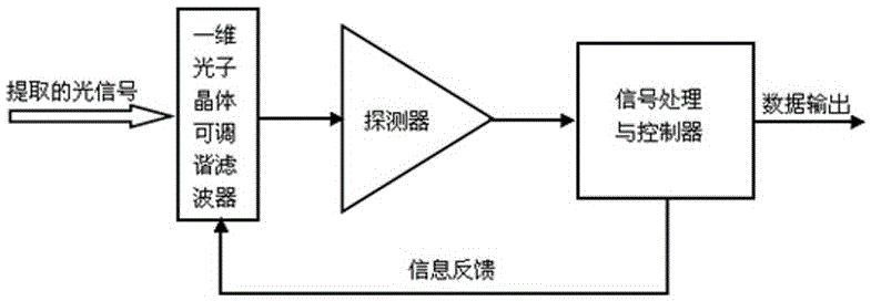
Tunable photonic crystal filters for optical network opm modules
A tuning filter and photonic crystal technology, applied in the field of optical communication, can solve the problems of large volume, channel interference, and low precision, and achieve the effect of reducing optical path, avoiding interference between channels, and reducing optical loss
- Summary
- Abstract
- Description
- Claims
- Application Information
AI Technical Summary
Problems solved by technology
Method used
Image

Examples
Embodiment 1
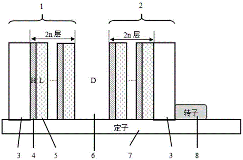
[0023] In this embodiment, the structure is (GaAs / MgF 2 ) 3 / Air / (GaAs / MgF 2 ) 3 As the core component of the OPM module, the tunable photonic crystal filter has a lattice constant of 397nm, the thickness of each layer of GaAs is 114nm, and the thickness of each layer of MgF 2 The layer thickness was 283 nm.
[0024] The growth of the photonic crystal needs the support of the substrate, and the two same first photonic crystal 1 and the second photonic crystal 2 constituting the filter are slightly different when grown on the substrate, and the growth sequence is reversed. Vacuum coating machine on SiO 2 A 114nm GaAs layer is deposited on the substrate 3, and then a 283nm MgF layer is deposited on the GaAs layer 2 layer, to obtain a cycle of the first photonic crystal 1, so that a total of 3 cycles of alternate deposition are completed to complete the preparation of the first photonic crystal 1; 2 Deposit 283nm MgF on substrate 3 2 layer, then the MgF 2 A GaAs layer of ...
Embodiment 2
[0027] In this embodiment, the structure is (GaAs / MgF 2 ) 4 / Air / (GaAs / MgF 2 ) 4 As the core component of the OPM module, the tunable photonic crystal filter has a lattice constant of 397 nm, a thickness of each GaAs layer of 114 nm, and each layer of MgF 2 The layer thickness is 283 nm.
[0028] Each of the first photonic crystal 1 and the second photonic crystal 2 needs to be deposited for 4 cycles, and the specific preparation method is the same as that in Embodiment 1.
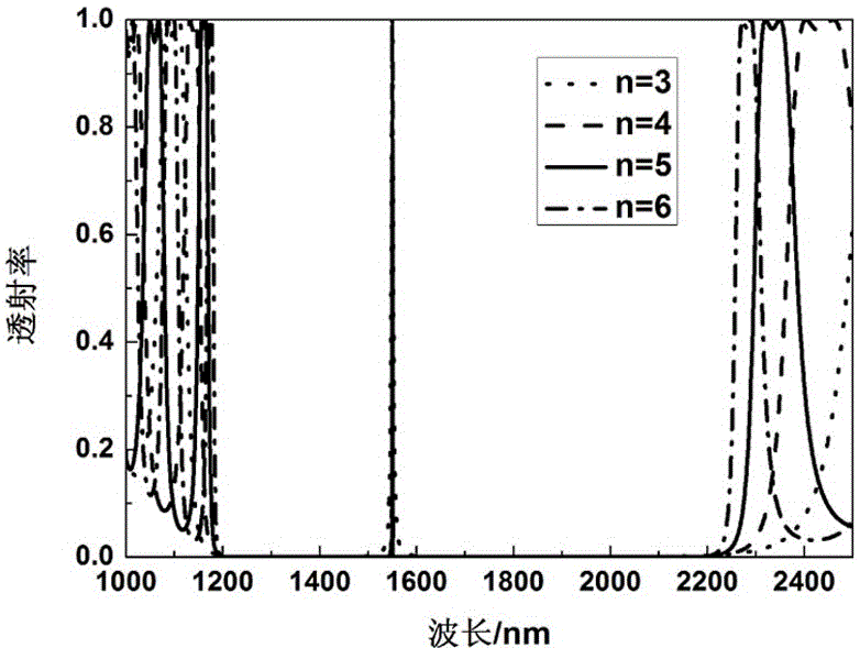
[0029] When the thickness of the air layer changes from 370.8 nm to 392.8 nm, such as Figure 5 , the corresponding transmission peak wavelength moves from 1533.276nm to 1556.138nm, the wavelength accuracy reaches 1 pm, and the transmittance is above 99%. Figure 8 It can be seen that the thickness of the air layer has a linear relationship with the peak wavelength, Figure 9 It shows that its average half maximum width is 0.7 nm.
Embodiment 3
[0031] In this embodiment, the structure is (GaAs / MgF 2 ) 5 / Air / (GaAs / MgF 2 ) 5 As the core component of the OPM module, the tunable photonic crystal filter has a lattice constant of 397 nm, a thickness of each GaAs layer of 114 nm, and each layer of MgF 2 The layer thickness is 283 nm.
[0032] The first photonic crystal 1 and the second photonic crystal 2 each need to be deposited for 5 cycles, and the specific preparation method is the same as that in Embodiment 1.
[0033] When the thickness of the air layer changes from 370.8 nm to 392.8 nm, such as Figure 6 , the corresponding transmission peak wavelength moves from 1533.2915nm to 1556.1331nm, the wavelength accuracy reaches 0.1 pm, and the transmittance is above 99%. Figure 8 It can be seen that the thickness of the air layer has a linear relationship with the peak wavelength, Figure 9 It shows that its average half maximum width is 0.12 nm.
PUM
 Abstract
Description
Claims
Application Information
 - Generate Ideas
- Intellectual Property
- Life Sciences
- Materials
- Tech Scout
- Unparalleled Data Quality
- Higher Quality Content
- 60% Fewer Hallucinations
Browse by: Latest US Patents, China's latest patents, Technical Efficacy Thesaurus, Application Domain, Technology Topic, Popular Technical Reports.
© 2025 PatSnap. All rights reserved.Legal|Privacy policy|Modern Slavery Act Transparency Statement|Sitemap|About US| Contact US: help@patsnap.com