Array substrate and manufacturing method of array substrate, and transflective display device
A technology of an array substrate and a manufacturing method, which is applied in the field of display, can solve the problems of low display brightness and low light transmittance of devices, and achieve the effect of improving display brightness and increasing transmittance
- Summary
- Abstract
- Description
- Claims
- Application Information
AI Technical Summary
Problems solved by technology
Method used
Image

Examples
Embodiment 1
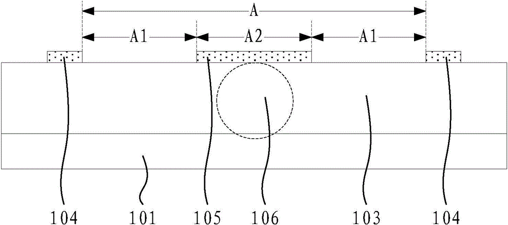
[0033] This embodiment provides an array substrate, the structure of the array substrate can be as follows figure 1 As shown, it includes: a base substrate 101 and a plurality of pixel units A located on the base substrate 101 , each pixel unit A includes: a transmissive area A1 and a reflective area A2 , and a reflective structure 105 is disposed in the reflective area A2 .
[0034] The above-mentioned array substrate 101 also includes: an optical element 106 disposed between the reflective structure 105 and the base substrate 101, the optical element 106 changes the propagation direction of the light incident from the back of the array substrate into the reflection area A2, so that the light from the The transmissive area A1 surrounding the reflective area A2 passes through.
[0035] In the array substrate provided in this embodiment, by setting the optical element 106 under the reflective structure 105, the optical element 106 can bypass the light incident on the reflective...
Embodiment 2
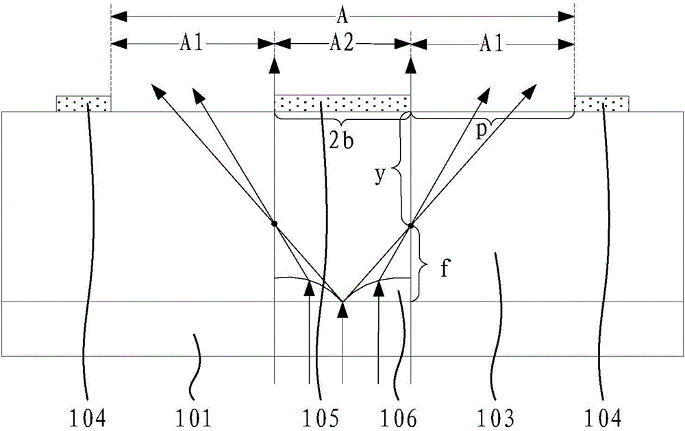
[0041] This embodiment provides an array substrate, the optical element 106 of which uses light refraction to make light bypass the reflective structure 105, and the structure of the array substrate can preferably be as follows figure 2As shown, the array substrate further includes: a flat layer 103 located between the optical element 106 and the reflective structure 105 . The structure of the optical element 106 preferably includes: a bottom surface that is flush with the side of the flat layer 103 close to the base substrate 101 and an arc surface opposite to the reflective structure 105; The side, that is, the curved surface is bent toward the base substrate 101; the refractive index of the optical element 106 is greater than that of the flat layer 103, so that light can be refracted toward the transmissive area A1.
[0042] When the light incident on the reflective area A2 from the back of the array substrate enters the flat layer 103 after passing through the optical ele...
Embodiment 3
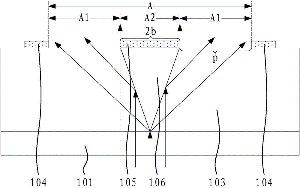
[0066] This embodiment provides an array substrate, the optical element 106 of which utilizes the reflection of light to make light bypass the reflective structure 105, and the structure of the array substrate can preferably be as follows image 3 As shown, the array substrate further includes: a flat layer 103 between the optical element 106 and the reflective structure 105, the flat layer 103 has a groove opening toward the reflected structure 105, and the optical element 106 is located in the groove; the optical element 106 includes a bottom surface overlapping with the reflective structure 105 and a reflective surface overlapping with an inner wall of the groove, and the reflective surface reflects light to the transmissive area A1.
[0067] When the light incident on the reflective area A2 from the back of the array substrate passes through the optical element 106 and enters the flat layer 103, since the reflective surface of the optical element 106 has the characteristics...
PUM
 Abstract
Description
Claims
Application Information
 - Generate Ideas
- Intellectual Property
- Life Sciences
- Materials
- Tech Scout
- Unparalleled Data Quality
- Higher Quality Content
- 60% Fewer Hallucinations
Browse by: Latest US Patents, China's latest patents, Technical Efficacy Thesaurus, Application Domain, Technology Topic, Popular Technical Reports.
© 2025 PatSnap. All rights reserved.Legal|Privacy policy|Modern Slavery Act Transparency Statement|Sitemap|About US| Contact US: help@patsnap.com