
Circuit structure for repair and flat panel display device having such circuit structure

A line structure, flat panel display technology, applied in the direction of circuits, nonlinear optics, static indicators, etc., can solve problems such as short circuits

Active Publication Date: 2018-08-28
SAMSUNG DISPLAY CO LTD
View PDF4 Cites 0 Cited by
  • Summary
  • Abstract
  • Description
  • Claims
  • Application Information

AI Technical Summary

Problems solved by technology

Therefore, in the event of defects such as particles or contamination during patterning photolithography, adjacent lines interposed with an interlayer insulating layer or lines crossing each other may be short-circuited to each other

Method used


Image

  • Circuit structure for repair and flat panel display device having such circuit structure
  • Circuit structure for repair and flat panel display device having such circuit structure
  • Circuit structure for repair and flat panel display device having such circuit structure

Examples


Embodiment Construction

[0020] Hereinafter, exemplary embodiments will be described in detail with reference to the accompanying drawings.

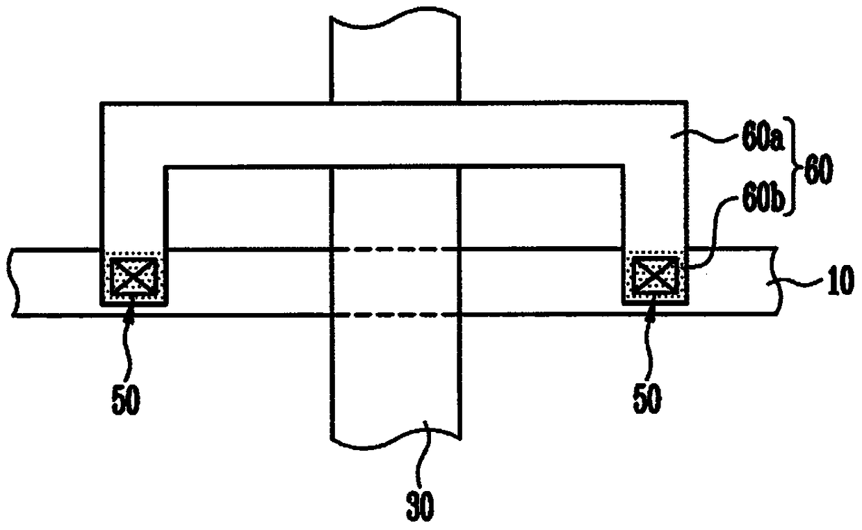
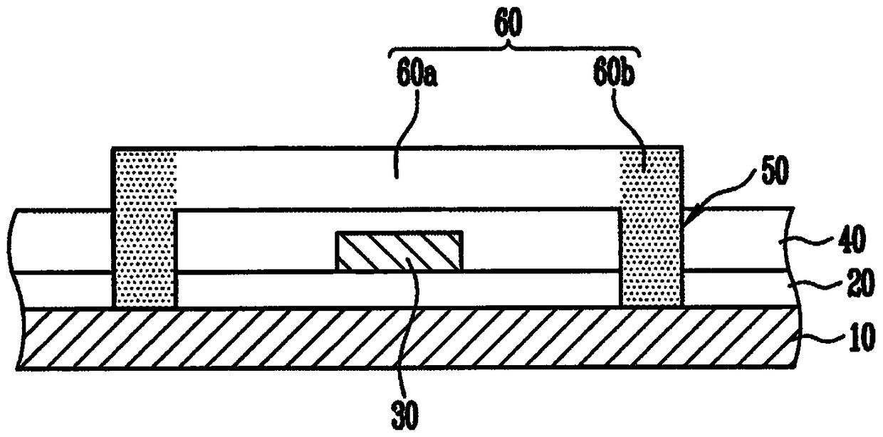
[0021] figure 1 and 2 are a plan view and a cross-sectional view showing a wiring structure according to one embodiment, respectively. refer to figure 1 , the first wiring 10 is formed to extend in one direction. The first line 10 may be a signal line for connecting devices or a power line for supplying power.

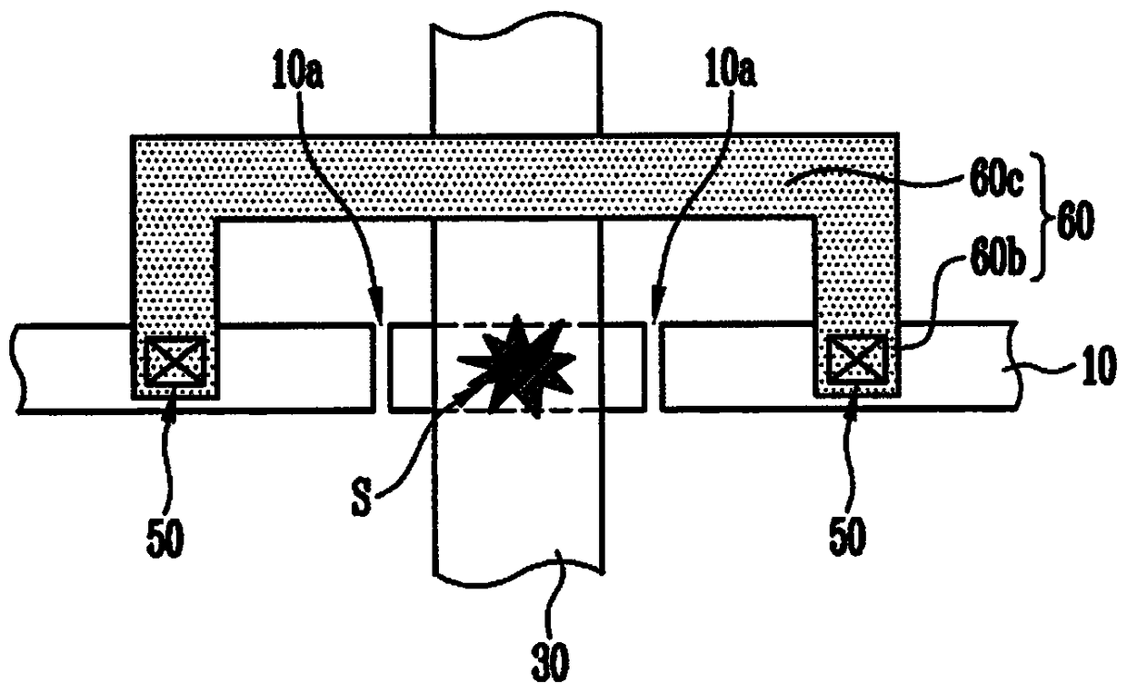
[0022] The second line 60 is formed parallel to the first line 10 . The second line 60 is provided at a predetermined portion of the first line 10 as a repair line. Both sides of the second line 60 are electrically connected to the first line 10 .

[0023] The third line 30 is formed to cross the first line 10 and the second line 60 . The third line 30 may be a signal line for connecting devices or a power line for supplying power.

[0024] refer to figure 1 and 2 , the second wiring 60 may be electrically insulated from the first wiring 10 by ...


PUM


Abstract

The invention relates to a circuit structure for repair and a flat panel display device with the circuit structure. A line structure for repair may include: a first line positioned in a first direction; a second line parallel to the first line, the second line having side portions extending from corresponding ends along the second direction and connected to the first line; and a third line crossing the first line and the second line, wherein at least a portion of the second line is made of undoped polysilicon.

Description

[0001] Cross references to related patent applications [0002] This application claims priority and benefit from Korean Patent Application No. 10-2013-0027563 filed with the Korean Intellectual Property Office on March 14, 2013, the entire contents of which are hereby incorporated by reference in their entirety. technical field [0003] Embodiments of the present invention relate to a wiring structure and a flat panel display device having such a wiring structure. Background technique [0004] Generally, a flat panel display device such as a liquid crystal display (LCD), a plasma display panel (PDP), or an organic light emitting display (OLED) is manufactured through a semiconductor device manufacturing process. In the semiconductor device manufacturing process, lines connecting thin film transistors, capacitors, and circuits are formed into patterns with extremely small widths and intervals, and the patterns are arranged in a multilayer structure with an interlayer insulat...

Claims


Application Information

Patent Timeline
Patent Type & Authority Patents(China)
IPC IPC(8): H01L23/50H01L27/32G02F1/13
CPCH01L23/525H01L2924/0002H01L23/5252H01L2924/00G09F9/00H01L21/28G09G3/20
Inventor 金炯秀郑根兑
Owner SAMSUNG DISPLAY CO LTD
Learn More