Off-chip accelerator applicable to fusion memory of 2.5D (2.5 dimensional) multi-core system

A multi-core system and memory technology, applied in the field of off-chip accelerator structure, can solve the problems of low communication efficiency and large communication delay between chips, and achieve the effect of avoiding design, avoiding performance and power loss, and reducing design complexity

Inactive Publication Date: 2014-09-10
FUDAN UNIV
View PDF4 Cites 5 Cited by
  • Summary
  • Abstract
  • Description
  • Claims
  • Application Information

AI Technical Summary

Problems solved by technology

[0004] The purpose of the present invention is to propose a 2.5D multi-core Implementation of o

Method used


Image

  • Off-chip accelerator applicable to fusion memory of 2.5D (2.5 dimensional) multi-core system
  • Off-chip accelerator applicable to fusion memory of 2.5D (2.5 dimensional) multi-core system
  • Off-chip accelerator applicable to fusion memory of 2.5D (2.5 dimensional) multi-core system

Examples


specific Embodiment approach

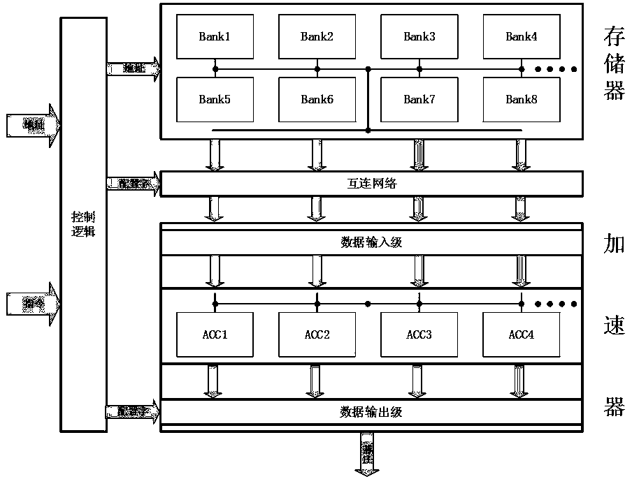
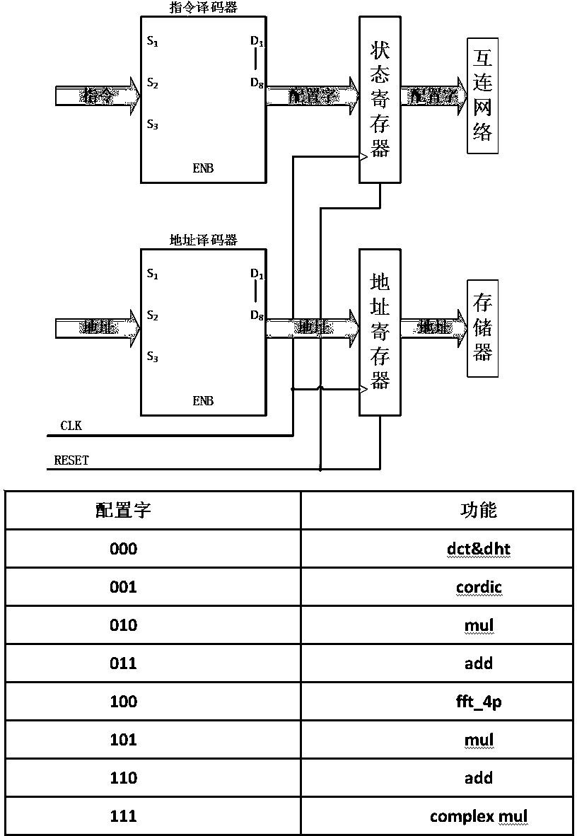
[0023] Such as figure 1 As shown, the structure of the fusion accelerator and memory proposed by the present invention is implemented on one chip in a highly integrated manner. The memory and the accelerator are connected together in a certain coupling way through interconnection. The processor sends data, address and configuration packets to the control logic through the interconnection channel between chips. The control logic decodes the configuration word according to the information in the instruction, and configures The word will be written into the status register immediately and saved, and it will be kept in the whole computing cycle until the arrival of the next configuration word. The output of the status register is directly connected to the interconnection network. The data in the memory flows along the configured interconnection network. You can choose to directly return to the processor without any processing, or you can choose to enter some kind of accelerator, ...


PUM


Abstract

The invention belongs to the technical field of multi-core processor design, in particular to an off-chip accelerator applicable to a fusion memory of a 2.5D (2.5 dimensional) multi-core system. The off-chip accelerator comprises a logic control circuit (comprising an instruction decoder and a state register), a memory (organized in an array manner), an accelerator and a configurable internetwork. The logic control circuit receives a configuration packet from a processor end, configures a corresponding link via analysis, and decides whether output data of the memory returns to a processor via acceleration logic. The accelerator is applicable to the specific application oriented 2.5D multi-core processing system, and can reduce performance loss due to longer inter-chip access delay, the output data of the memory can be calculated and output by selecting different acceleration units, and the accelerator has certain flexibility.

Description

technical field [0001] The invention belongs to the technical field of multi-core processors, and in particular relates to an off-chip accelerator structure of a fusion memory oriented to specific applications. Background technique [0002] In recent years, in order to solve the increasingly complex problem of single-chip design, people have gradually shifted their attention to the design and implementation of 2.5D and 3D circuits. A common form is to separate the processor, memory and accelerator on different chips. accomplish. However, for multimedia applications with intensive storage and repeated calculations, the data communication from the memory to the processor and accelerator needs to go through the I / O port of the chip and the interconnection channel between the chips to reach the destination chip, and then along the The same path back to memory, sometimes even data communication across multiple chips. In this case, in the implementation process, there will be tw...

Claims


Application Information

Patent Timeline
IPC IPC(8): G06F13/16
Inventor 虞志益朱世凯林杰周炜周力君
Owner FUDAN UNIV
Why Eureka
Try Eureka