Eureka AIR delivers breakthrough ideas for toughest innovation challenges, trusted by R&D personnel around the world.

Silicon wafer separating device

A substrate and negative pressure technology, which is applied in the field of silicon wafer processing equipment, can solve problems such as unfavorable fragmentation, water reduction, and negative pressure adsorption efficiency, and achieve the effects of improving work efficiency, improving adsorption force, and reliable structure

Active Publication Date: 2014-09-03
ZHANGJIAGANG ULTRASONIC & ELECTRIC
View PDF6 Cites 3 Cited by
  • Summary
  • Abstract
  • Description
  • Claims
  • Application Information

AI Technical Summary

Problems solved by technology

[0002]Before inserting silicon wafers, the stacked silicon wafers must be sliced ​​first, and because the silicon wafers are light and fragile, and the adjacent silicon wafers There is a certain adsorption force between them, so we choose to divide the pieces in water. When dividing the pieces, negative pressure adsorption is generally used to realize the separation and transportation. This will cause part of the water in the tank to be drawn out with the negative pressure, which will cause the water tank The continuous reduction of water in the film is not conducive to fragmentation. In addition, it will also affect the efficiency of negative pressure adsorption.

Method used


Image

  • Silicon wafer separating device
  • Silicon wafer separating device

Examples


Embodiment Construction

[0014] Below in conjunction with the embodiment shown in the accompanying drawings, the present invention is described in detail as follows:

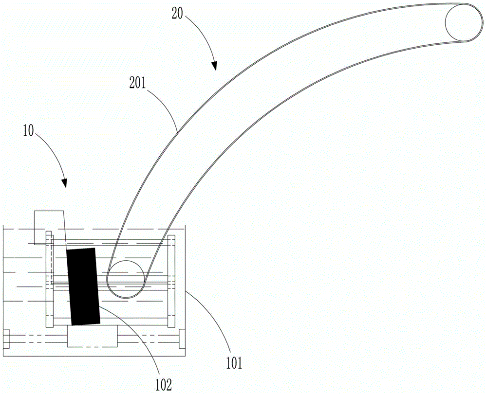
[0015] as attached figure 1 and attached figure 2 As shown, a slicer device includes a feeding unit 10, a suction unit 20 and a negative pressure unit 30. The feeding unit 10 is arranged in a water tank 101, wherein, the feeding unit 10 is placed with There is a substrate stack 102 of a plurality of substrates, each substrate is arranged along a substantially vertical plane; the suction unit 20 includes a conveyor belt 201, and the conveyor belt 201 is provided with a number of negative pressure adsorption holes communicated with a negative pressure power source, Conveyor belt 201 has part to be arranged in water tank 101 and this part extends to feeding unit 10, when substrate pile 102 is advanced along feeding direction, the substrate in substrate pile 102 can be one by one by the negative on conveyer belt 201. The pressure a...


PUM


Abstract

The invention discloses a silicon wafer separating device which comprises a feeding unit, a suction unit and a negative pressure unit. The negative pressure unit comprises a negative pressure box, at least one air suction hole formed in the negative pressure box, a sealing box body, an air suction pump and an infusion pump, wherein the air suction pump and the infusion pump are connected with the sealing box body. The air suction holes are communicated to the sealing box body. Negative pressure suction holes are communicated with the negative pressure box. The negative pressure box is partially located inside a water groove. At least one air suction hole is located above the position close to the water surface in the water groove. According to the silicon wafer separating device, silicon wafers are separated in water and are sucked and conveyed through negative pressure power, gas and liquid are separated by the sealing box body, the air suction pump and the infusion pump, the air suction pump and the infusion pump are connected with the sealing box body, water obtained after separation is sent back into the water groove so as to keep the water amount in the water groove for facilitating silicon wafer separation, the negative pressure pumping space in the sealing box body is ensured, then the suction force of the negative pressure suction holes is improved, meanwhile, the negative pressure pumping volume in the negative pressure box can be utilized to the large extent, the negative pressure working efficiency is improved, the structure is reliable, and the silicon wafer separating device is suitable for application and popularization.

Description

technical field [0001] The invention relates to a silicon chip processing equipment, in particular to a slicing device for slicing underwater. Background technique [0002] Before inserting the silicon wafers, the stacked silicon wafers should be divided into slices. Since the silicon wafers are light and fragile, and there is a certain amount of adsorption between adjacent silicon wafers, the slices are chosen to be divided in water. When slicing, negative pressure adsorption is generally used to achieve slicing and transportation, which will cause part of the water in the tank to be pumped out with the negative pressure, which will cause the water in the tank to decrease continuously, which is not conducive to slicing. In addition, it will also Affect the efficiency of negative pressure adsorption. Contents of the invention [0003] In view of the above-mentioned technical deficiencies, the purpose of the present invention is to provide a slicing device, which can separ...

Claims


Application Information

Patent Timeline
Patent Type & Authority Applications(China)
IPC IPC(8): B65H3/12
Inventor 陈宏
Owner ZHANGJIAGANG ULTRASONIC & ELECTRIC
Why Eureka
Eureka Blog
Learn More