
Method for manufacturing LED light source

A technology of LED light source and manufacturing method, which is applied to semiconductor devices, electrical components, circuits, etc., can solve the problems of high cost, complex heat dissipation design, and many process flows, and achieve the effect of reducing material cost and simplifying production process flow.

Inactive Publication Date: 2014-08-06
宋勇飞
View PDF3 Cites 54 Cited by
  • Summary
  • Abstract
  • Description
  • Claims
  • Application Information

AI Technical Summary

Problems solved by technology

[0003] At present, there are two methods for manufacturing LED light sources: method 1, packaging the LED chip into a plug-in or patch lamp bead, and then assembling the lamp bead, circuit board, heat sink, power supply, housing and other materials into an LED lamp; method 2. Directly fix the LED chip on the metal or ceramic substrate with a printed circuit layer, then wire welding, dispensing, and curing to form an LED light-emitting module, and then connect the LED light-emitting module to the circuit board, heat sink, power supply, housing and other materials Assembled into LED lamps; method 1 requires two packaging processes of lamp bead packaging and LED lamp assembly to manufacture LED lamps, with many technological processes, high cost, and complicated heat dissipation design; method 2 manufactures LED lamps, although the LED lamp bead packaging process is omitted. However, there are more manufacturing processes of aluminum substrates (or ceramic substrates) with circuit board printing layers, and the process flow is a bit more, radiators are still required, and the cost is also high

Method used


Image

  • Method for manufacturing LED light source
  • Method for manufacturing LED light source
  • Method for manufacturing LED light source

Examples


Embodiment Construction

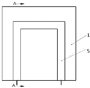
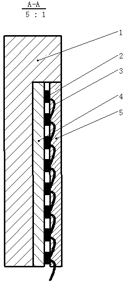
[0017] figure 1 , figure 2 Respectively, a schematic structural view and a cross-sectional view of the LED light source module of the present invention, figure 1 Shown is a schematic diagram after the manufacture is completed, the glass plate 1 on the surface and the fluorescent glue 5 on the surface of the groove of the glass plate 1 can be seen; figure 2 As shown in the A-A direction sectional view, the internal structure of the LED light source module of the present invention can be seen, according to figure 2 The manufacturing method described in the present invention is described as follows:

[0018] (a) casting glass plate 1 with grooves in glass;

[0019] (b) Apply fluorescent glue 4 on the bottom of the groove of the glass plate 1;

[0020] (c) Fix a row of LED chips 2 (usually blue chips) on the fluorescent glue 4 at equal intervals;

[0021] (d) connecting the electrodes of the LED chips 2 in series with gold wires 3;

[0022] (e) Coat another layer of fluor...


PUM


Abstract

A method for manufacturing an LED light source is characterized by sequentially comprising the following steps that (a) a substrate is made of transparent materials, wherein a groove is formed in the surface of the substrate; (b) the bottom of the groove is coated with fluorescent gum; (c) an LED chip is fixed to the fluorescent gum at the bottom of the groove; (d) electrodes of the LED chip are connected in series by a metal wire; (e) the LED chip and the metal wire are coated with fluorescent gum. According to the method for manufacturing the LED light source, a traditional manufacturing process of an LED light source is simplified and material consumption is reduced.

Description

technical field [0001] The invention relates to the field of LED light sources, in particular to a method for manufacturing an LED light source. Background technique [0002] LED is a kind of semiconductor light source, which has the advantages of energy saving, small size and long life. In recent years, it has gradually replaced traditional incandescent lamps and will become the main lighting source in the future. [0003] At present, there are two methods for manufacturing LED light sources: method 1, packaging the LED chip into a plug-in or patch lamp bead, and then assembling the lamp bead, circuit board, heat sink, power supply, housing and other materials into an LED lamp; method 2. Directly fix the LED chip on the metal or ceramic substrate with a printed circuit layer, then wire welding, dispensing, and curing to form an LED light-emitting module, and then connect the LED light-emitting module to the circuit board, heat sink, power supply, housing and other materials...

Claims


Application Information

Patent Timeline
Patent Type & Authority Applications(China)
IPC IPC(8): H01L33/48H01L33/62H01L33/64
CPCH01L33/486H01L33/644H01L2933/0075H01L2933/0033H01L2924/181H01L2224/45144H01L2224/48091H01L2224/48137H01L2924/00014H01L2924/00012H01L2924/00
Inventor 宋勇飞
Owner 宋勇飞
Learn More