Array substrate, preparation method of array substrate and display panel

An array substrate and cross-section technology, which is applied in nonlinear optics, instruments, optics, etc., can solve the problems of abnormal tapping, failure to return to the original position in time, light leakage of the display panel, etc., and achieve the effect of reducing light leakage.

Inactive Publication Date: 2014-08-06
BOE TECH GRP CO LTD +1
View PDF5 Cites 11 Cited by
  • Summary
  • Abstract
  • Description
  • Claims
  • Application Information

AI Technical Summary

Problems solved by technology

But if the area of ​​the contact end of the spacer and the spacer pillow is too small, new problems will occur again, such as figure 2 as shown, figure 2 It is a structural schematic diagram of a display panel in the prior art when a contact problem occurs. When the surface of the display panel is subjected to external pressure F, the color filter substrate 01 will have a certain offset relative to the array substrate 03. When the offset exceeds a certain distance, That is, when the spacer 02 provided on the color filter substrate 01 deviates beyond the supporting edge of the spacer cushion 04 provided on the array substrate 03, after the external force F disappears, the spacer 02 is blocked by the wiring level difference of the array substrate 03. If it cannot or cannot be restored to the original position in time, it will cause light leakage on the display panel. In terms of technology, this bad phenomenon is called Touch Mura.

Method used


Image

  • Array substrate, preparation method of array substrate and display panel
  • Array substrate, preparation method of array substrate and display panel
  • Array substrate, preparation method of array substrate and display panel

Examples


Embodiment 1

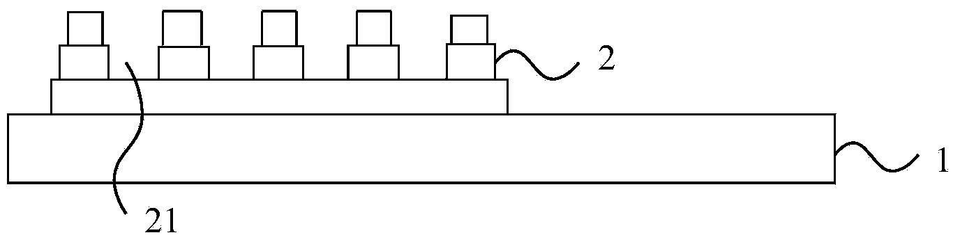
[0042] image 3 A schematic diagram of the structure of the array substrate provided for the embodiment of the present invention, such as image 3 As shown, the array substrate provided by the embodiment of the present invention includes: a spacer pillow 2 for supporting a spacer, and the supporting end of the spacer pillow 2 is provided with at least one concave portion 21 .

[0043] The array substrate provided by the embodiment of the present invention is applied in a display panel, such as Figure 4 as shown, Figure 4 The schematic diagram of the display panel structure provided by the embodiment of the present invention, the array substrate 1 and the color filter substrate 3 are connected in pairs, the spacer pillow 2 corresponds to the spacer 4 and is used to support the spacer 4, through the array The support end of the spacer pillow 2 provided on the substrate 1 is provided with one or more recesses 21, which can increase the size of the support end of the spacer pi...

Embodiment 2

[0053] An embodiment of the present invention provides a method for preparing an array substrate, including:

[0054] Coating photoresist on the substrate on which the semiconductor layer and the source-drain metal layer have been formed, and performing the first etching to form a spacer pillow;

[0055] A second etch is performed on the spacer pillow, forming a depression on the support end of the spacer pillow.

[0056] In the method for preparing an array substrate provided by the embodiment of the present invention, a spacer pillow provided with at least one groove is formed at the same time as the semiconductor layer and the source-drain metal layer are formed. During the preparation process, there is no need to purchase new ones separately. The mask plate does not need to add new materials, and it will not affect the display effect of the display panel.

[0057] Such as Figure 8a ~ Figure 8i as shown, Figures 8a-8i It is a schematic structural diagram during the pre...

Embodiment 3

[0069] An embodiment of the present invention provides a display panel, such as Figure 4 As shown, it includes a color filter substrate, and also includes the array substrate described in any one of the first embodiment above.

[0070] Based on the above advantages of the array substrate, the display panel provided by the embodiment of the present invention has a better display effect.


PUM


Abstract

The invention discloses an array substrate, a preparation method of the array substrate and a display panel. The array substrate comprises a plurality of spacer pads for supporting spacers, wherein the supporting end of each spacer pad is provided with at least one concave portion. The array substrate is applied to the display panel, the array substrate is connected with a color film substrate, and the spacer pads correspond to the spacers in a one-to-one mode and are used for supporting the spacers; the supporting end of each spacer pad arranged on the array substrate is provided with one or more concave portions, and the size of the supporting end of each spacer pad can be increased, namely the spacers arranged on the color film substrate can move in a larger range on the spacer pads but the contact area of each spacer and the corresponding spacer pad cannot be increased; meanwhile, by means of the arrangement of the concave portions, friction force between the spacers and the spacer pads can be increased, the spacers can be prevented from deviating when the display panel bears external pressure, and the light leaking phenomenon of the display panel is reduced.

Description

technical field [0001] The invention relates to the technical field of displays, in particular to an array substrate, a method for preparing the array substrate and a display panel. Background technique [0002] Existing display panels are mainly composed of polarizers, array substrates, color filter substrates, liquid crystal layers, and the like. The regular arrangement of the liquid crystal layer can realize color display. The thickness of the liquid crystal layer affects the transmittance of light injected into the liquid crystal panel. When the transmittance is inconsistent, the display will be uneven. Therefore, in order to achieve a uniform display of the display panel, it is very important to ensure a uniform thickness of the liquid crystal layer (cell thickness). . [0003] In the manufacture of liquid crystal display panels, such as figure 1 as shown, figure 1 It is a schematic structural diagram of a display panel in the prior art, and a spacer 02 is usually a...

Claims


Application Information

Patent Timeline
Patent Type & Authority Applications(China)
IPC IPC(8): G02F1/1339G02F1/1333
Inventor 周波宋勇志
Owner BOE TECH GRP CO LTD
Why Eureka
Try Eureka