Deposition of silicon oxide by atmospheric pressure chemical vapor deposition
A silicon oxide and silicon oxide-containing technology, used in organic chemistry, gaseous chemical plating, chemical instruments and methods, etc., can solve the problems of contamination of coating equipment and low deposition efficiency.
- Summary
- Abstract
- Description
- Claims
- Application Information
AI Technical Summary
Problems solved by technology
Method used
Image
Examples
example 1
[0063] Example 1: Deposition of SiO from n-octylsilane precursor + air 2
[0064] The n-octylsilane was evaporated with 4.5 standard liters (slm) of nitrogen carrier heated to 180° C. per minute. The vaporized n-octylsilane stream was then combined with 6.5 slm of dry air heated to 180°C and delivered as a single stream onto the soda lime silica glass substrate surface. The soda lime silica glass substrate was pre-coated with 170 nm of tin oxide and heated to 625°C-650°C. Optical characterization after deposition showed about 390 nm of silicon dioxide formed at a deposition rate of 6.5 nm / s.
[0065] NOTE: The SiO 2 Deposited on a tin oxide (high refractive index) coated glass to contribute to the optical characteristics of the resultant layer. In practice, the SiO 2 Can be deposited directly on a glass substrate.
example 3
[0068] Example 3: Deposition of SiO from n-hexylsilane precursor + air 2
[0069] The same experiment as provided in Example 1 was repeated using n-hexylsilane as the alkylsilane precursor instead of n-octylsilane. Optical characterization after deposition showed the formation of about 350 nm of silicon dioxide at a deposition rate of 6 nm / s.
example 4
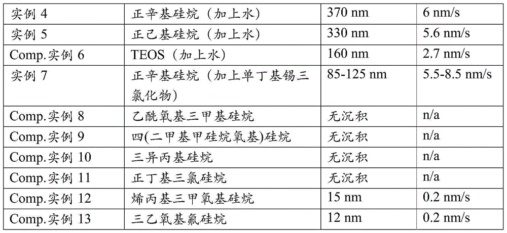
[0070] Example 4: Deposition of SiO from n-octylsilane precursor + air and water 2
[0071] The same experiment was repeated as provided in Example 1 using n-octylsilane as the evaporated precursor, but water was also added to the precursor mixture. Specifically, the conditions of Example 1 were repeated by adding about a 1:1 molar ratio of water to silicon precursor. Optical characterization after deposition showed that about 370 nm of silicon dioxide was deposited at a rate of 6 nm / s.
PUM
| Property | Measurement | Unit |
|---|---|---|
| thickness | aaaaa | aaaaa |
| thickness | aaaaa | aaaaa |
| thickness | aaaaa | aaaaa |
Abstract
Description
Claims
Application Information
 - R&D Engineer
- R&D Manager
- IP Professional
- Industry Leading Data Capabilities
- Powerful AI technology
- Patent DNA Extraction
Browse by: Latest US Patents, China's latest patents, Technical Efficacy Thesaurus, Application Domain, Technology Topic, Popular Technical Reports.
© 2024 PatSnap. All rights reserved.Legal|Privacy policy|Modern Slavery Act Transparency Statement|Sitemap|About US| Contact US: help@patsnap.com


