Circuit board

A circuit board and line technology, applied in the direction of printed circuit components, etc., can solve the problems of lower transmission quality, impedance mismatch, low impedance, etc., and achieve the effect of improving high-frequency transmission quality and consistent impedance

Inactive Publication Date: 2014-07-02
HONG FU JIN PRECISION IND (SHENZHEN) CO LTD +1
View PDF4 Cites 7 Cited by
  • Summary
  • Abstract
  • Description
  • Claims
  • Application Information

AI Technical Summary

Problems solved by technology

Thinner lines have higher impedance and thicker lines have lower impedance, which will cause impedance mismatch and reduce transmission quality

Method used


Image

  • Circuit board
  • Circuit board
  • Circuit board

Examples


Embodiment Construction

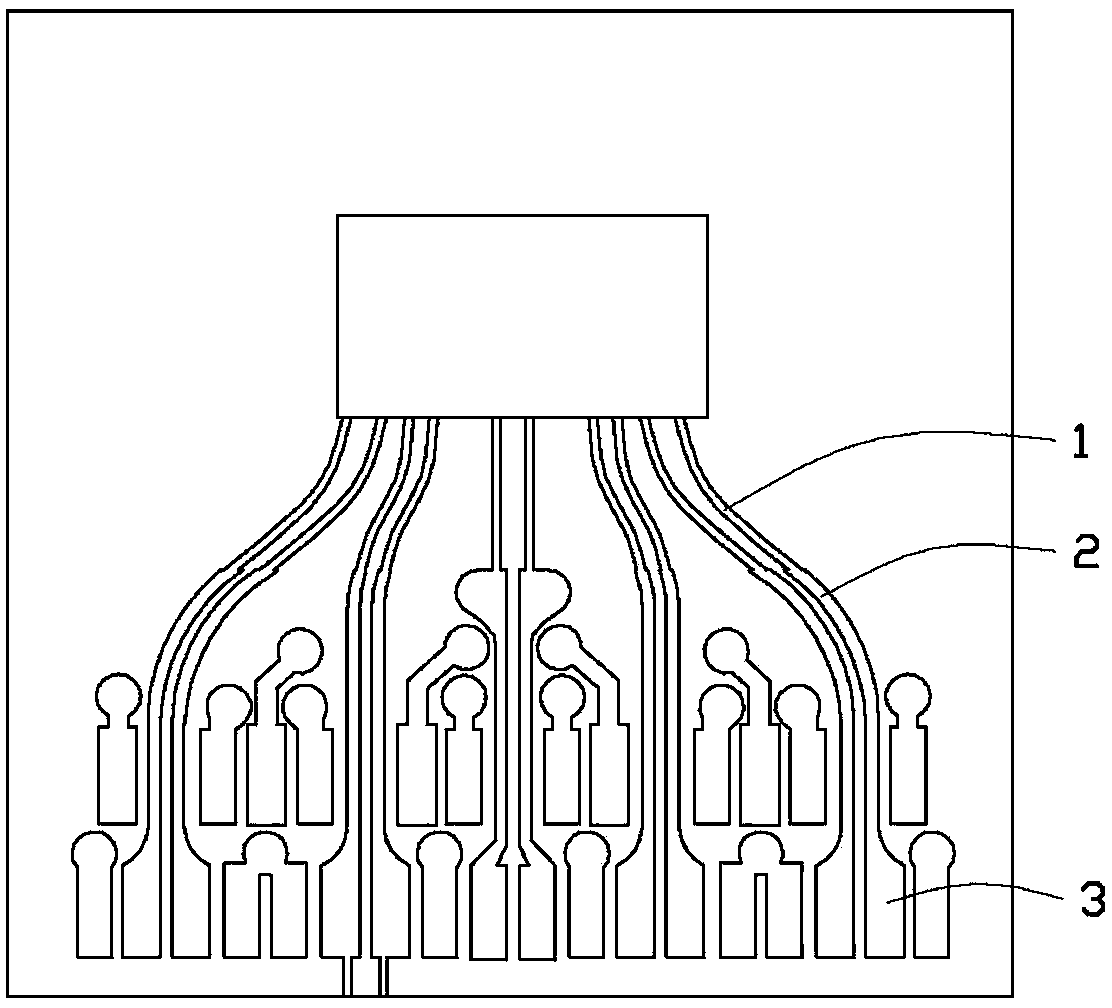
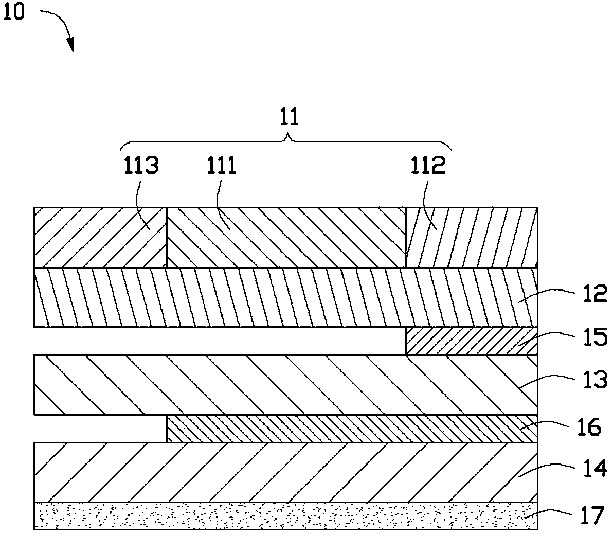
[0014] see figure 2 The circuit board 10 provided by the first embodiment of the present invention includes a signal wiring layer 11, a first dielectric layer 12, a second dielectric layer 13, a third dielectric layer 14, a first ground layer 15, a second ground layer 16 and the third ground layer 17, the first dielectric layer 12, the first ground layer 15, the second dielectric layer 13, the second ground layer 16, the third dielectric layer 14 and the third ground layer 17 gradually move away from the signal traces Line layer 11.

[0015] In practical applications, the circuit board 10 also includes a conductive layer, etc., for simplicity, figure 1 Only the signal wiring layer 11, the first dielectric layer 12, the second dielectric layer 13, the third dielectric layer 14, the first ground layer 15, the second ground layer 16 and the The third ground layer 17 .

[0016] The signal trace layer 11 and the first ground layer 15 are respectively located on two opposite sur...


PUM


Abstract

A circuit board comprises a signal routing layer, a first dielectric layer, a first grounding layer, a second dielectric layer, a second grounding layer, a third dielectric layer and a third grounding layer. The first dielectric layer, the first grounding layer, the second dielectric layer, the second grounding layer, the third dielectric layer and the third grounding layer are gradually far away from the signal routing layer. The signal routing layer comprises a signal line, a chip circuit and a connector circuit. The first grounding layer is arranged correspondingly to the chip circuit; the second grounding layer is arranged correspondingly to the signal line; and the third grounding layer is arranged correspondingly to the connector circuit.

Description

technical field [0001] The invention relates to a circuit board, in particular to an impedance matching circuit board. Background technique [0002] In the Light Peak system specification, it is expected to achieve at least a single channel 10Gb / s speed. In such a high-frequency transmission system, impedance matching is particularly important. If the impedance does not match, it will cause a lot of energy loss. Increasing the bit error rate may even cause EMI problems, so impedance matching design is very important in high-frequency systems. [0003] The Light Peak system converts electrical signals into optical signals through photoelectric conversion and then transmits them over long distances. However, wiring of electrical signals is unavoidable. Usually, when designing high-frequency lines, the impedance is designed to be 50 ohms single-ended. Or differential 100 ohms. [0004] like figure 1 As shown, there are IC position 1, middle position 2 and connector position ...

Claims


Application Information

Patent Timeline
Patent Type & Authority Applications(China)
IPC IPC(8): H05K1/02
Inventor 吴开文
Owner HONG FU JIN PRECISION IND (SHENZHEN) CO LTD
Why Eureka
Try Eureka