Wafer level applied RF shields

A wafer-level, wafer-based technology, applied in the fields of magnetic/electric field shielding, semiconductor/solid-state device components, semiconductor devices, etc.

Inactive Publication Date: 2014-06-11
HUATIAN TECH KUNSHAN ELECTRONICS
View PDF5 Cites 0 Cited by
  • Summary
  • Abstract
  • Description
  • Claims
  • Application Information

AI Technical Summary

Problems solved by technology

Additionally, surface mount RF shielding can create warpage in the overall chip package shape

Method used


Image

  • Wafer level applied RF shields
  • Wafer level applied RF shields
  • Wafer level applied RF shields

Examples


Embodiment Construction

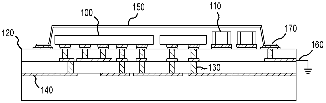
[0021] The present invention provides a low cost method for wafer level application of RF shielding used in multiple electronic packaging formats and applications. The method is particularly useful in embedded die packaging applications to provide high throughput RF shielding for wafer level applications.

[0022] figure 1 A typical EMI shielding system on a printed wiring board (PWB) is shown. Single or multiple active and / or passive components 100 together with surface mounted discrete components 110 may be used to form an electronic system. The components are mounted on a typical printed circuit or wiring board 120 . Electrical connections between components are made through vias 130 and redistribution traces 140 using a standard PWB. A typical SMT board mount RF shield 150 covers the system components and is connected to electrical ground 160 through the PWB circuit. The RF shield is typically welded or glued to the PWB around the perimeter of component 170 .

[0023]...


PUM


Abstract

An embodiment of a method of forming an on-chip RF shield on an integrated circuit chip in accordance with the present disclosure includes providing a wafer level integrated circuit component wafer having a front side and a back side before singulation; applying a resin metal layer on a back side of the wafer; and then separating the wafer into discrete RF shielded components. It is this resin metal layer on the back side that acts effectively as the RF shield, after singulation, i.e. separation of the wafer, into discrete RF shielded components.

Description

[0001] Cross References to Related Applications [0002] This application claims the benefit of priority to U.S. Provisional Patent Application No. 61 / 546,862, filed October 13, 2011, entitled "Wafer Level Applied RF Shields," the U.S. The disclosure of the provisional patent application is incorporated herein by reference in its entirety. technical field [0003] The present invention relates generally to the formation of a semiconductor chip, and more particularly, to a structure and method of formation for an on-chip RF shield for an embedded wafer Packaged active, passive or discrete components. Background technique [0004] In some electronic packaging applications, devices and system circuits must be protected from sources of electromagnetic interference (EMI). It is also important to ensure that the device or system circuitry does not emit EMI radiation to systems external to it. Thereby, the ability of such a system to operate as intended in a particular electroma...

Claims


Application Information

Patent Timeline
Patent Type & Authority Applications(China)
IPC IPC(8): H01L23/60H05K9/00
CPCH01L2924/14H01L2224/0401H01L2924/01029H01L2224/16225H01L23/552H01L2224/32225H01L2924/19105H01L2224/73253H01L2224/93H01L24/93H01L2924/15192H01L2224/11H01L2224/27
Inventor 克拉克·戴维西奥多·G·特斯耶尔
Owner HUATIAN TECH KUNSHAN ELECTRONICS
Why Eureka
Try Eureka