An electrochemical reaction cell for dark-field microscopic observation
A technology of electrochemical reaction and chemical reaction, applied in the field of electrochemistry, can solve problems such as difficult to achieve long-term use, poor reusability, complex device integration, etc., and achieve the effects of low cost, simple production, and convenient operation
- Summary
- Abstract
- Description
- Claims
- Application Information
AI Technical Summary
Problems solved by technology
Method used
Image
Examples
Embodiment 1
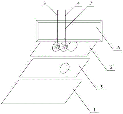
[0019] figure 1 It is a structural schematic diagram of the present invention, as shown in the figure, an electrochemical reaction cell that can be used for dark field microscopic observation, including an electrochemical reaction cell and an electrochemical element, wherein the electrochemical reaction cell is made of ITO glass An insulating thin layer-2 with holes is installed on the sheet 1, and the holes on the insulating thin layer-2 are two and the two holes are connected; the electrochemical element includes a counter electrode 3 and a reference electrode 4, and the counter electrode 3 and the reference electrode 4 are respectively positioned and installed in the holes on the insulating thin layer-2. The hole on the insulating thin layer is the space for receiving the sample. Further, the insulating thin layer-2 is a polydimethylsiloxane thin layer, or other materials such as non-conductive high polymers. Since the insulating thin layer is very thin, low-height operat...
Embodiment 2
[0024] This example illustrates the fabrication of the device.
[0025] Preparation of PDMS thin-layer cover sheet: Sylgard184 monomer and curing agent are mixed in a ratio of 10:1 (mass ratio), degassed, poured on a clean plane cofferdam, heat-cured, and then peeled off to obtain it. Hole punching.
[0026] Design and manufacture PDMS (polydimethylsiloxane) film; cover the cured PDMS with a round hole on the ITO glass treated by plasma; adhere the PDMS thin layer with three notched holes to the above On the PDMS thin layer, the first notch hole of this layer is aligned with the hole on the PDMS thin layer of the first layer. The reaction cell was then fixed under a dark-field microscope.
[0027] After the glass and PDMS were cleaned separately, they were placed in a plasma cleaner for 2 minutes, and then aligned and bonded immediately.
[0028] Preparation of the electrode positioning device: spirally coil the bottom ends of the counter electrode and the reference electro...
PUM
 Abstract
Description
Claims
Application Information
 - R&D
- Intellectual Property
- Life Sciences
- Materials
- Tech Scout
- Unparalleled Data Quality
- Higher Quality Content
- 60% Fewer Hallucinations
Browse by: Latest US Patents, China's latest patents, Technical Efficacy Thesaurus, Application Domain, Technology Topic, Popular Technical Reports.
© 2025 PatSnap. All rights reserved.Legal|Privacy policy|Modern Slavery Act Transparency Statement|Sitemap|About US| Contact US: help@patsnap.com


