Method and structure for controlling via hole impedance of PCB board

A technology of PCB board and impedance control, which is applied in the field of communication to achieve high precision and improve the effect of signal quality

Active Publication Date: 2018-05-18
NEW H3C TECH CO LTD
View PDF4 Cites 0 Cited by
  • Summary
  • Abstract
  • Description
  • Claims
  • Application Information

AI Technical Summary

Problems solved by technology

[0004] In view of this, the present invention proposes a novel via impedance control technology on the basis of the conventional via impedance control technology in the industry, which can greatly improve the defects of the existing via impedance control technology, thereby improving the overall network communication. Purpose of Signal Quality

Method used


Image

  • Method and structure for controlling via hole impedance of PCB board
  • Method and structure for controlling via hole impedance of PCB board
  • Method and structure for controlling via hole impedance of PCB board

Examples


Embodiment Construction

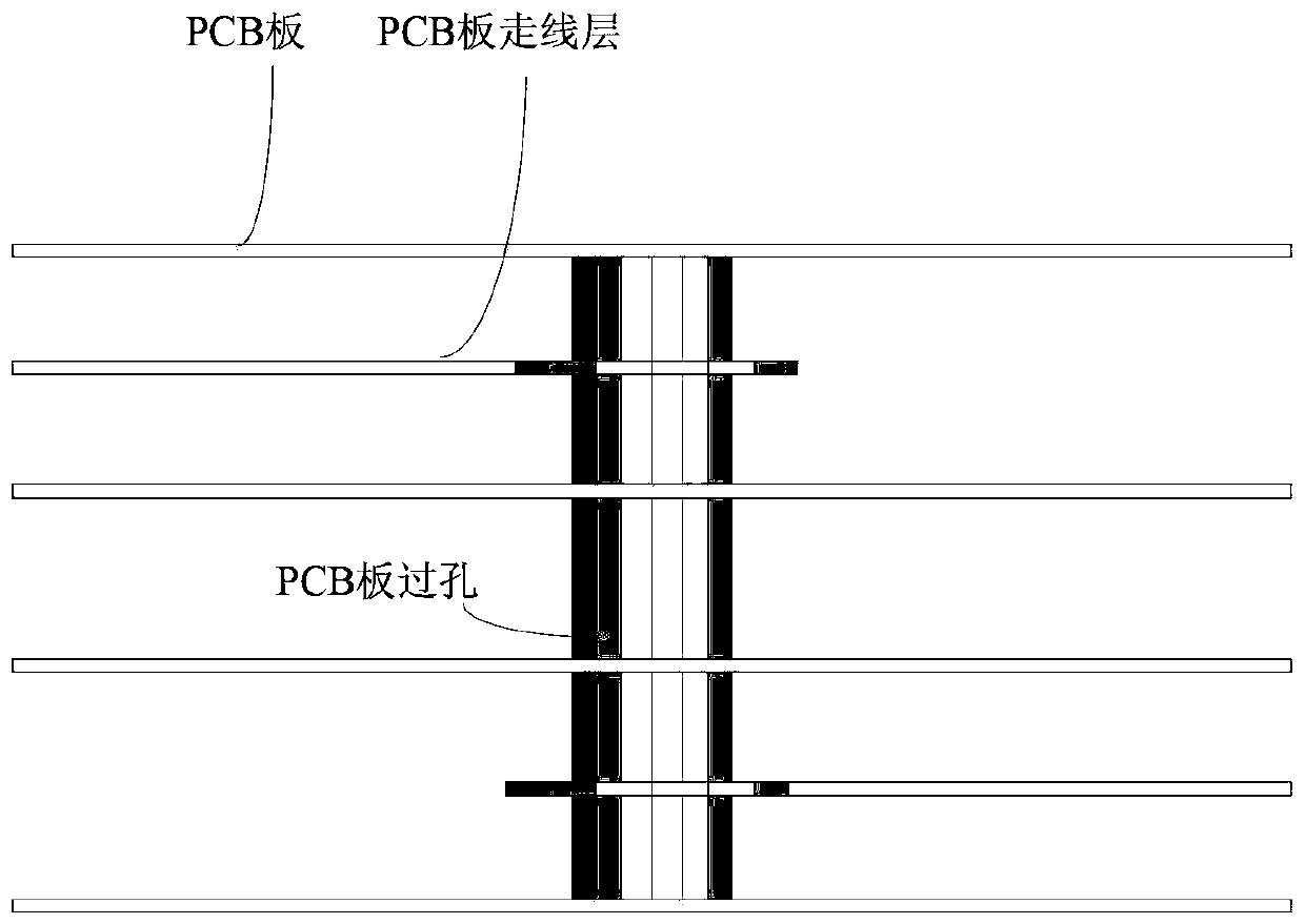
[0024] still with figure 2 Take the PCB board shown as an example, the production of signal vias on the PCB board generally includes the following control indicators:

[0025] 1. Drill Diamater

[0026] 2. Plating thickness (Plated)

[0027] 3. Regular Pad

[0028] 4. Thermal Relief

[0029] 5. Anti Pad (Anti Pad)

[0030] Among them, ordinary pads are mainly used in the outgoing layer and surface layer of the PCB board. The ordinary pads in the outgoing layer can enhance the mechanical connection performance between PCB traces and metal vias, which is beneficial to PCB mechanical processing. The ordinary pads of other layers except the surface layer and the outgoing layer are called non-functional pads. According to the signal integrity theory, the non-functional pad acts as the stub of the communication link, which will affect the effective transmission of the signal. The standard practice in the industry for many years is to delete the non-functional pads between the...


PUM


Abstract

The invention discloses a method and a structure for controlling the impedance of PCB board through holes. By reusing the non-functional pads on the PCB that are discarded by the industry, set non-functional pads on other layers other than the outgoing layer connected to the vias to adjust the balance of the metal pads on the via transmission path, thereby improving Consistency of distributed capacitance per unit length. The present invention can greatly improve the defects of the current via hole impedance control technology, so as to achieve the purpose of improving the overall network communication signal quality of the PCB board.

Description

technical field [0001] The invention relates to the technical field of communications, in particular to a method and structure for controlling the impedance of PCB via holes. Background technique [0002] PCB (Printed Circuit Board) board is an important part of communication equipment, and it is the support body of electronic components and the provider of electrical connection. As the electronic signal rate of the communication carried by the PCB board is getting higher and higher, the electronic circuits on the PCB board need to be controlled in impedance to ensure the quality of the electronic signal. By adjusting the stacking design and line width of each layer of the PCB board, precise control of different impedance values ​​​​of the PCB board lines can be achieved. At present, a common practice in the industry is to control according to 50Ω for single-ended traces and 100Ω for differential traces. The impedance control technology of PCB traces is very mature. The t...

Claims


Application Information

Patent Timeline
Patent Type & Authority Patents(China)
IPC IPC(8): H05K3/40
Inventor 李孝群
Owner NEW H3C TECH CO LTD
Why Eureka
Try Eureka