Double-sided adhesive film and manufacturing method thereof
A manufacturing method, double-sided adhesive technology, applied in the direction of adhesives, film/sheet adhesives, etc., can solve the problem of uneven appearance of stretched films
- Summary
- Abstract
- Description
- Claims
- Application Information
AI Technical Summary
Problems solved by technology
Method used
Image
Examples
Embodiment 1)
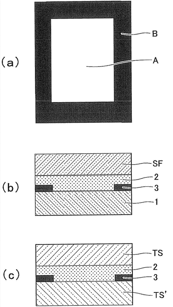
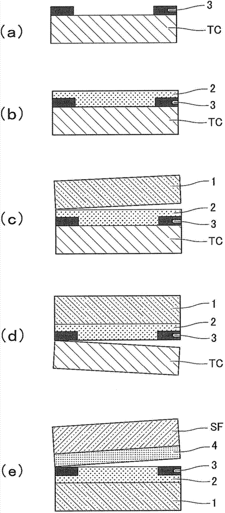
[0087] refer to Figure 7 (a) First, as a release film to be the temporary support body TC, a 50-μm-thick PET film (manufactured by Fujimori Industries: DG2.5) provided with a silicon release layer was prepared. Silver mirror paint (manufactured by Seiko Advance Ltd.: Chrome Silver 300MR) was screen-printed on the release surface, and dried at 100° C. for 5 minutes to form a logo pattern with a film thickness of 1 μm. Black paint (made by Teikoku Ink Co., Ltd.: GLS-HF919-ink) was screen-printed thereon, dried at 100°C for 5 minutes, and the decorative layer 3 having a frame-like pattern of a black layer with a film thickness of 10 μm was laminated on the temporary support TC on (process (i)). The decorative layer 3 thus formed is provided on a portion corresponding to the outer peripheral portion of the display portion of the display panel, and the inside of the decorative layer 3 having the frame-like pattern corresponds to the display portion of the display panel.
[0088]...
Embodiment 2)
[0094] As in Example 1, a logo pattern was formed. Black paint (made by Imperial Ink: GLS-HF919-ink + strengthening agent for GSL glass = 100wt% + 0.5wt%) was screen-printed on it, dried and heat-cured at 90°C for 30 minutes, and a black layer with a film thickness of 10 μm was laminated. The decorative layer 3 is formed on a portion corresponding to the outer peripheral portion of the display portion of the display panel.
[0095] Next, isobutyl acrylate having a weight average molecular weight (Mw) of 400,000 was dissolved in ethyl acetate so as to have a solid content of 30 wt%, to prepare a coating material for an adhesive layer. Using an applicator, the paint was applied so that the film thickness of the display part was 20 μm to cover the decorative layer 3 and the temporary support TC, and dried at 100° C. for 2 minutes to form the first adhesive layer 2 .
[0096] After laminating a PET film with a silicon release layer (manufactured by Teijin DuPont: A31, thickness: ...
Embodiment 3)
[0099] In the same manner as in Example 1, an adhesive sheet with a decorative layer formed to the first adhesive layer 2 was produced. As a film with an adhesive layer, a tape (manufactured by Nitto Denko: CS6661T) in which a 25 μm thick adhesive layer (second adhesive layer 4) is formed on a 50 μm thick PET film with a silicon release layer was used , on the surface of the adhesive sheet with a decorative layer peeled off the release film (DG2.5) of the temporary support, the adhesive layer of the film with an adhesive layer is laminated closely, and a die-cutting die with a large blade is used Cut to a size of 60 mm x 120 mm to make a double-sided adhesive film.
[0100] Next, using this double-sided adhesive film, a display panel was formed by the same method as in Example 1.
PUM
| Property | Measurement | Unit |
|---|---|---|
| thickness | aaaaa | aaaaa |
| thickness | aaaaa | aaaaa |
| thickness | aaaaa | aaaaa |
Abstract
Description
Claims
Application Information
 - R&D
- Intellectual Property
- Life Sciences
- Materials
- Tech Scout
- Unparalleled Data Quality
- Higher Quality Content
- 60% Fewer Hallucinations
Browse by: Latest US Patents, China's latest patents, Technical Efficacy Thesaurus, Application Domain, Technology Topic, Popular Technical Reports.
© 2025 PatSnap. All rights reserved.Legal|Privacy policy|Modern Slavery Act Transparency Statement|Sitemap|About US| Contact US: help@patsnap.com


