Multiaxial capacitive accelerometer and acceleration detection method
An accelerometer and capacitive technology, applied in the field of micro-electromechanical structures, can solve the problems of temperature drift and impact resistance performance that cannot meet the requirements, and achieve the effects of reducing deformation, improving sensitivity, and reducing temperature drift
- Summary
- Abstract
- Description
- Claims
- Application Information
AI Technical Summary
Problems solved by technology
Method used
Image
Examples
Embodiment 1
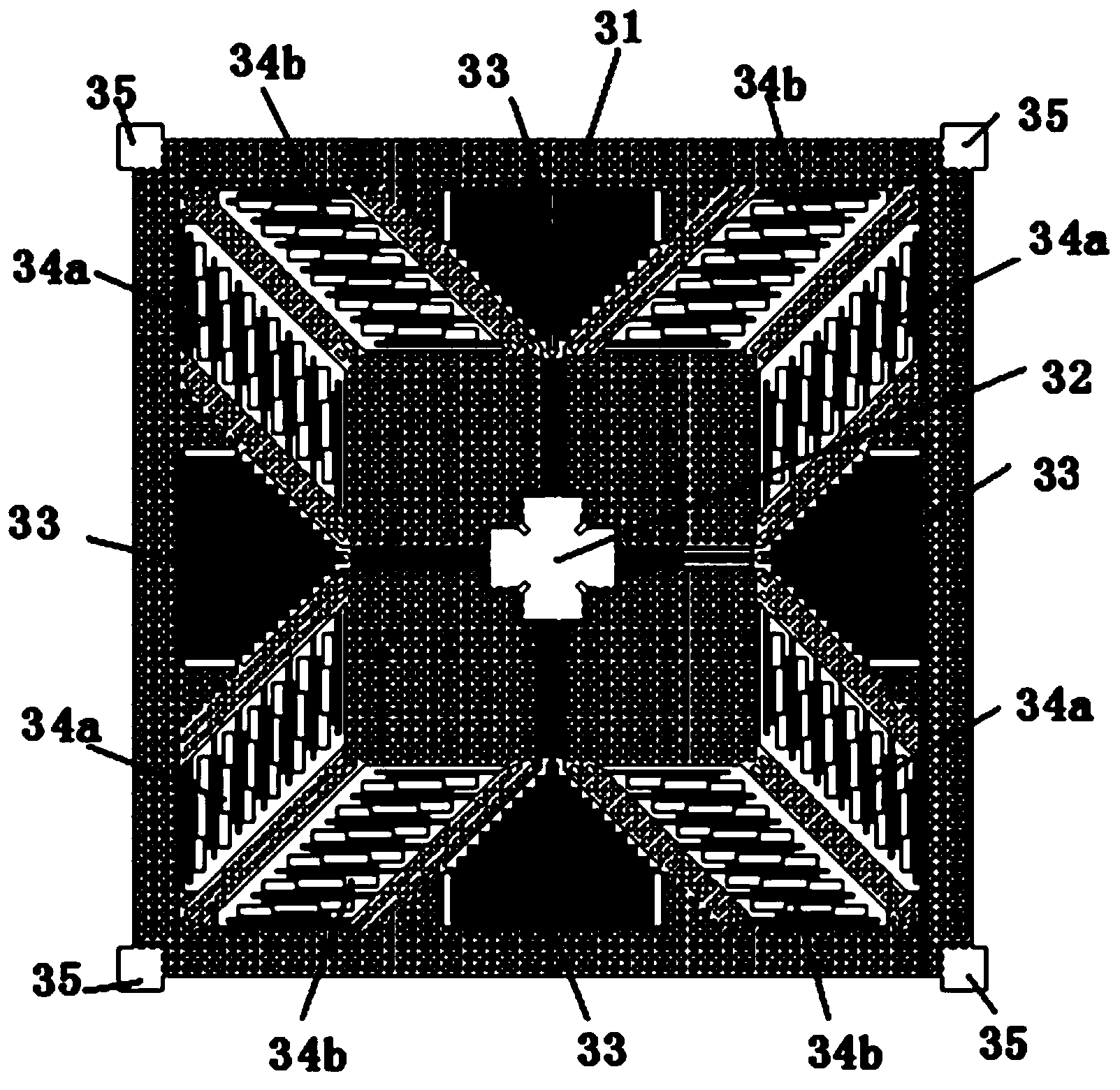
[0039] The multi-axis capacitive accelerometer of this embodiment is a two-axis capacitive accelerometer, that is, X and Y axis accelerometers. figure 1 It is the overall schematic diagram of the multi-axis capacitive accelerometer of this embodiment. Such as figure 1 As shown, the multi-axis capacitive accelerometer includes a substrate ( figure 1 Not shown) and an XY-axis structure layer, the XY-axis structure layer includes a movable mass 31, a central anchor point 32, an elastic structure 33, and detection electrodes 34a, 34b.
[0040] Continue to refer figure 1 In this embodiment, the XY axis structure layer 1a includes a total of eight detection electrodes, and the eight detection electrodes are symmetrically distributed at the four vertex corners of the movable mass 31. This placement method effectively utilizes the chip area and is beneficial to increase acceleration. The sensitivity of the meter. In detail, four detection electrodes 34a are symmetrically distributed on t...
Embodiment 2
[0049] The multi-axis capacitive accelerometer in this embodiment is a three-axis capacitive accelerometer, that is, it includes the X- and Y-axis accelerometers as described in the first embodiment, and also includes a Z-axis accelerometer. Specific as Image 6 As shown, the X and Y-axis accelerometers include an XY-axis structure layer 1a, and the Z-axis accelerometer includes torsion-type Z-axis structure layers 1b, 1c located on both sides of the XY-axis structure layer 1a, and the XY-axis structure The layer 1a has a square shape as a whole, and the Z-axis structure layers 1b and 1c have a rectangular shape as a whole to save area as much as possible.
[0050] Figure 7 Yes Image 6 A schematic cross-sectional view along line a when the substrate of the structure shown is warped, Figure 8 Yes Image 6 Schematic diagram of the middle Z-axis structure layer 1b. Such as Figure 6 to Figure 8 As shown, the Z-axis structure layer 1b, 1c includes: movable masses 17, 18, fixed an...
PUM
 Abstract
Description
Claims
Application Information
 - R&D
- Intellectual Property
- Life Sciences
- Materials
- Tech Scout
- Unparalleled Data Quality
- Higher Quality Content
- 60% Fewer Hallucinations
Browse by: Latest US Patents, China's latest patents, Technical Efficacy Thesaurus, Application Domain, Technology Topic, Popular Technical Reports.
© 2025 PatSnap. All rights reserved.Legal|Privacy policy|Modern Slavery Act Transparency Statement|Sitemap|About US| Contact US: help@patsnap.com


