Common Mode Signal Filter
A common-mode signal and filter technology, applied in the field of thin-film common-mode signal filters, can solve the problems of complex structure, increased manufacturing cost, and many process variables, and achieve the effect of eliminating common-mode noise and accurately controlling common-mode impedance.
- Summary
- Abstract
- Description
- Claims
- Application Information
AI Technical Summary
Problems solved by technology
Method used
Image
Examples
no. 1 example 〕
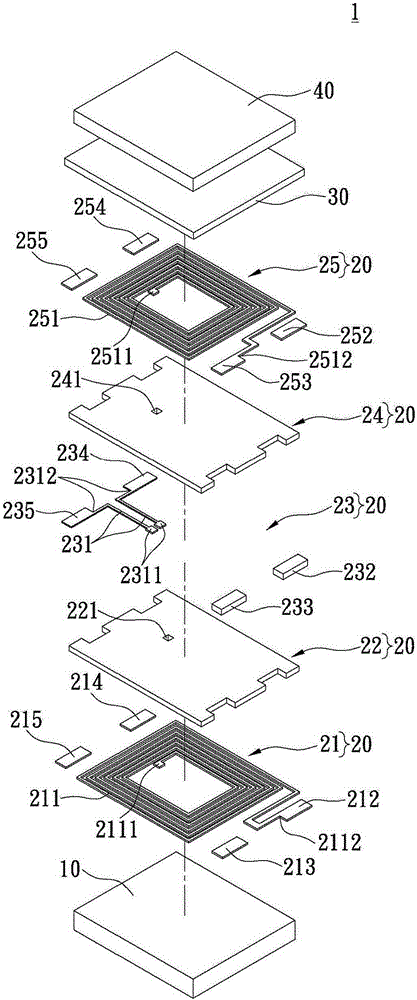
[0108] see figure 1 , which shows an exploded view of the common-mode signal filter 1 of the first embodiment of the present invention. The common mode signal filter 1 includes a non-magnetic insulating substrate 10 , a coil stack structure 20 , an insulating layer 30 and a magnetic material layer 40 .
[0109] Specifically, the coil stack structure 20 is disposed on the non-magnetic insulating substrate 10, and the coil stack structure 20 sequentially includes a first coil body layer 21, a first electrical insulation layer 22, and a coil lead-out layer 23. , a second electrical insulation layer 24 and a second coil body layer 25 . Wherein the insulating layer 30 is disposed between the coil stack structure 20 and the magnetic material layer 40, so that the magnetic material layer 40 is applied on the coil stack structure 20 to become the cover of the common-mode signal filter 1, which can increase the common-mode signal filtering The inductance effect of device 1. In this ...
no. 2 example
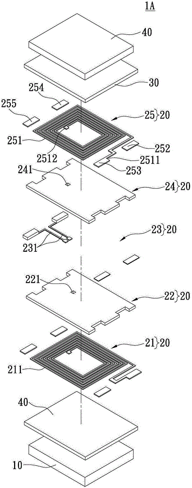
[0122] see Figure 3A , which shows an exploded view of the common-mode signal filter 1A of the second embodiment of the present invention. The difference from the first embodiment is that the common mode signal filter 1A further includes another magnetic material layer 40, and the another magnetic material layer 40 is disposed on the coil stack structure 20 and the non-magnetic insulating substrate Between 10.
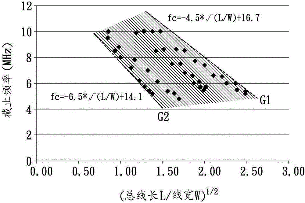
[0123] More specifically, the magnetic material layer 40 is interposed between the first coil body layer 21 and the non-magnetic insulating substrate 10 to achieve a higher common-mode noise filtering effect. Similarly, the bus length L (mm) and line width W (mm) of the first coil 211 and the second coil 251 can satisfy the following relational expression:
[0124] [(14.1-fc) / 6.5] 2 2 , where fc is the cutoff frequency of the differential mode signal, and the cutoff frequency is approximately between 4 and 10 MHz, which meets the requirements of specific portable e...
no. 3 example
[0126] see Figure 3B , which shows an exploded view of the common-mode signal filter 1B of the third embodiment of the present invention. The difference from the second embodiment is that the common mode signal filter 1B further includes a plurality of magnetic parts 50 . Specifically, these magnetic parts 50 are ferrite cores (Ferrite core), which have the advantages of high magnetic permeability, high resistance and small eddy current loss in a wide frequency range.
[0127]In addition, the first electrical insulation layer 22 and the second electrical insulation layer 24 are provided with a through hole 222 , 242 , and the through hole 222 and the through hole 242 are respectively adjacent to the first conductive structure 221 and the second conductive structure 241 . Thereby, these magnetic parts 50 can be arranged on the inner side of the first coil 211, one end of the pair of L-shaped wires 231 and the inner side of the second coil 251 through the through holes 222, 24...
PUM
 Abstract
Description
Claims
Application Information
 - Generate Ideas
- Intellectual Property
- Life Sciences
- Materials
- Tech Scout
- Unparalleled Data Quality
- Higher Quality Content
- 60% Fewer Hallucinations
Browse by: Latest US Patents, China's latest patents, Technical Efficacy Thesaurus, Application Domain, Technology Topic, Popular Technical Reports.
© 2025 PatSnap. All rights reserved.Legal|Privacy policy|Modern Slavery Act Transparency Statement|Sitemap|About US| Contact US: help@patsnap.com


