TSV process method without metal CMP
A process method and metal technology, applied in the field of metal-free CMP TSV process, can solve the problems of high barrier layer cost, expensive CMP equipment, no mention of metal-free CMPTSV process, etc., to reduce costs, lower industrialization threshold and The effect of manufacturing costs
- Summary
- Abstract
- Description
- Claims
- Application Information
AI Technical Summary
Problems solved by technology
Method used
Image
Examples
Embodiment Construction
[0043] The present invention will be further described below in conjunction with specific drawings and embodiments.
[0044] A TSV process method free of metal CMP, comprising the following steps:
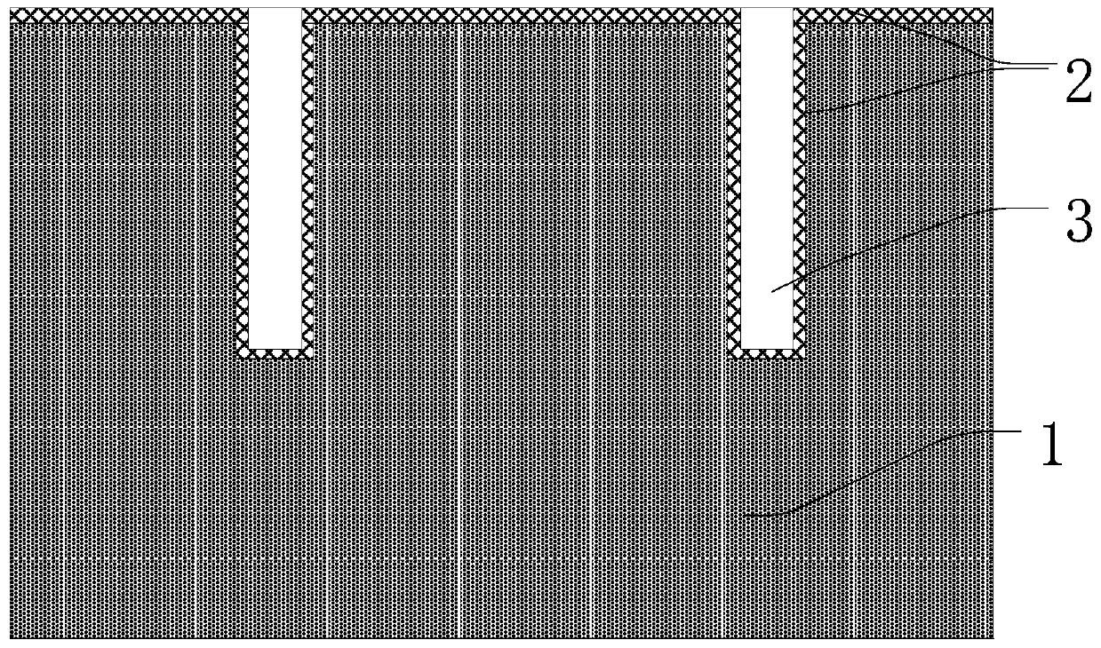
[0045] S1. If figure 1 As shown, a wafer 1 is provided as a substrate, a blind hole 3 (TSV hole) is formed in the wafer 1 by a deep reactive ion etching process, and an insulating layer 2 is formed on the upper surface of the wafer 1 and the inner wall of the blind hole 3 ;
[0046] The depth and diameter of the blind hole 3 can be determined according to specific requirements, and the aspect ratio is generally not less than 3:1. The material of the insulating layer 2 may be materials such as silicon dioxide, silicon nitride, silicon oxynitride, organic polymer, etc., and the layer structure may be a one-layer or multi-layer structure of the above materials.
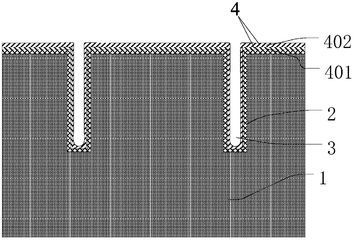
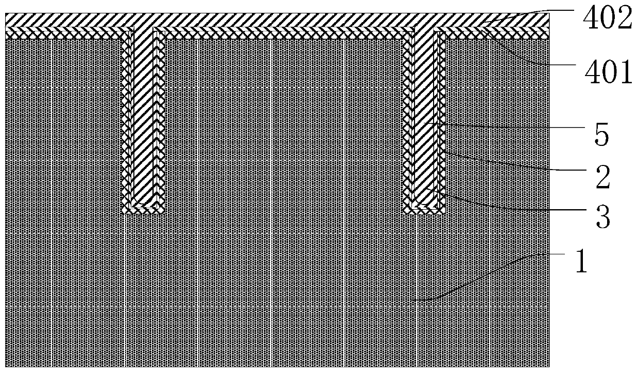
[0047] S2. If figure 2 As shown, a barrier layer 401 and a seed layer 402 are deposited on the upper surface of the wa...
PUM
 Abstract
Description
Claims
Application Information
 - R&D Engineer
- R&D Manager
- IP Professional
- Industry Leading Data Capabilities
- Powerful AI technology
- Patent DNA Extraction
Browse by: Latest US Patents, China's latest patents, Technical Efficacy Thesaurus, Application Domain, Technology Topic, Popular Technical Reports.
© 2024 PatSnap. All rights reserved.Legal|Privacy policy|Modern Slavery Act Transparency Statement|Sitemap|About US| Contact US: help@patsnap.com


