
Groove-type Schottky power device structure and method for manufacturing same

A technology of power devices and manufacturing methods, applied in the field of trench-type Schottky power device structures and their manufacturing, can solve problems that are difficult to improve, and achieve improved endurance and antistatic capabilities, low leakage, and bidirectional optimization of operating characteristics Effect

Active Publication Date: 2013-12-18
CHINA RESOURCES MICROELECTRONICS (CHONGQING) CO LTD
View PDF4 Cites 4 Cited by
  • Summary
  • Abstract
  • Description
  • Claims
  • Application Information

AI Technical Summary

Problems solved by technology

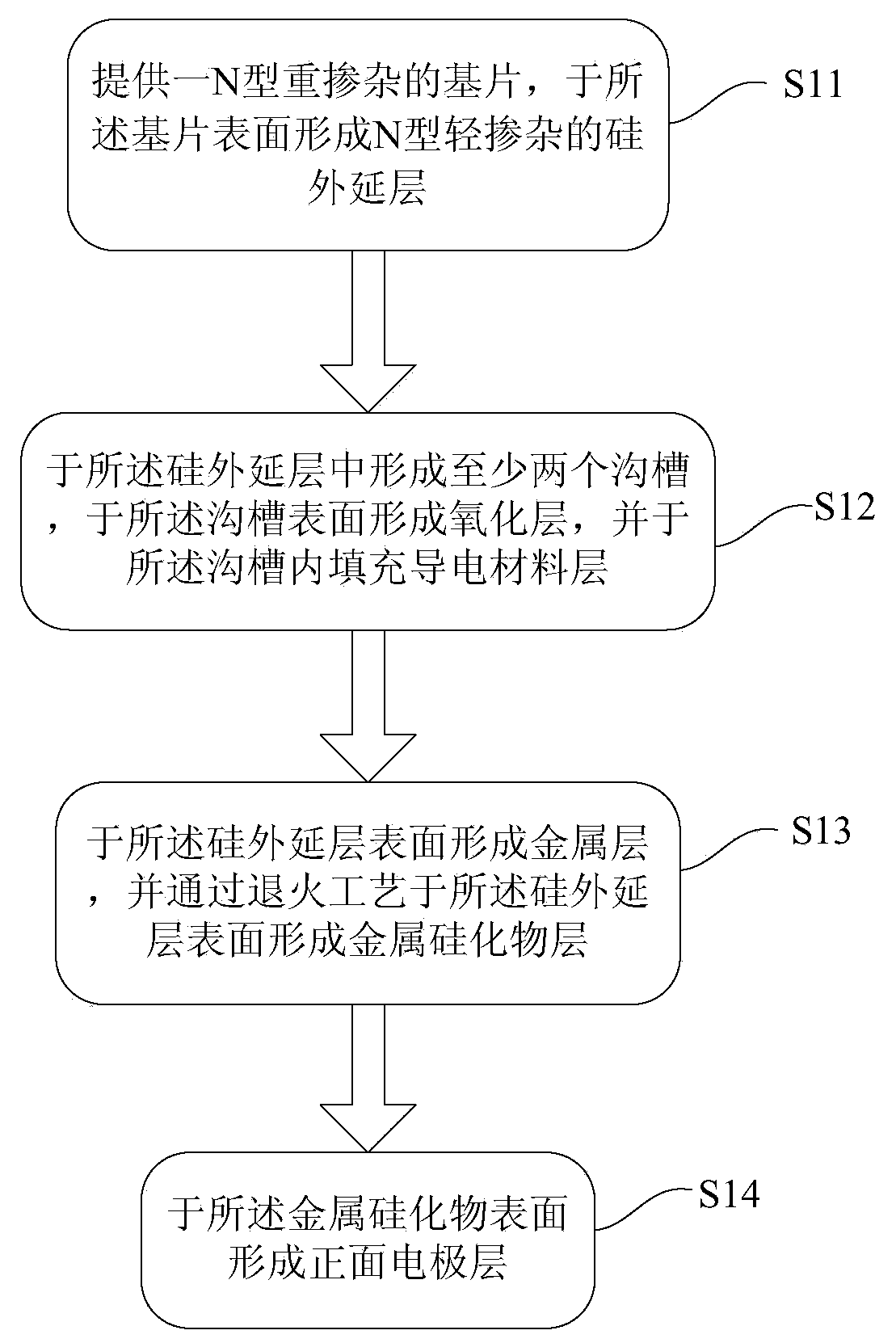
[0006] In view of the above-mentioned shortcomings of the prior art, the purpose of the present invention is to provide a method for manufacturing a trench-type Schottky power device structure, which is used to solve the difficulty in improving the forward voltage drop of the Schottky power device in the prior art. The problem

Method used


Image

  • Groove-type Schottky power device structure and method for manufacturing same
  • Groove-type Schottky power device structure and method for manufacturing same
  • Groove-type Schottky power device structure and method for manufacturing same

Examples


Embodiment 2

[0089] like Figure 1 to Figure 9 and Figure 11 As shown, this embodiment provides a method for manufacturing a trench Schottky power device structure, the basic steps of which are the same as those of TiN / Ti / Ni / Ag stack, that is, the front electrode is TiN layer 108 , AlSi layer 201 , Ti layer 110 , TiN layer 111 , Ti layer 112 , Ni layer 113 , and Ag layer 114 in order from bottom to top.

[0090] like Figure 11 As shown, this embodiment also provides a trench-type Schottky power device structure, the basic structure of which is the same as that of Embodiment 1, wherein the front electrode is TiN / AlSi / Ti / TiN / TiN / AlSi / TiN / TiN / Ti / Ni / Ag stack, that is, the front electrode is TiN layer 108 , AlSi layer 201 , Ti layer 110 , TiN layer 111 , Ti layer 112 , Ni layer 113 , and Ag layer 114 in order from bottom to top.

Embodiment 3

[0092] like Figure 1 to Figure 9 and Figure 12 As shown, this embodiment provides a method for manufacturing a trench Schottky power device structure, the basic steps of which are the same as those in Embodiment 1, wherein the front electrode is TiN / Al / Ti / TiN / Al / Ti / TiN / Ti / Ni / Ag stack, that is, the front electrode is TiN layer 108 , Al layer 301 , Ti layer 110 , TiN layer 111 , Ti layer 112 , Ni layer 113 , and Ag layer 114 in order from bottom to top.

[0093] like Figure 12 As shown, this embodiment also provides a trench-type Schottky power device structure, the basic structure of which is the same as that of Embodiment 1, wherein the front electrode is TiN / Al / Ti / TiN / TiN / Al / TiN / TiN / Ti / Ni / Ag stack, that is, the front electrode is TiN layer 108 , Al layer 301 , Ti layer 110 , TiN layer 111 , Ti layer 112 , Ni layer 113 , and Ag layer 114 in order from bottom to top.

[0094]As mentioned above, the present invention provides a trench type Schottky power device structure...


PUM

PropertyMeasurementUnit
thicknessaaaaaaaaaa
widthaaaaaaaaaa
depthaaaaaaaaaa

Abstract

The invention provides a groove-type Schotty power device structure and a method for manufacturing the groove-type Schotty power device structure. The groove-type Schotty power device structure comprises an N-type heavily doped substrate, an N-type slightly doped silicone epitaxial layer, at least two grooves, conductive material layers, a metal silicide layer and a positive electrode layer, wherein the N-type slightly doped silicone epitaxial layer is arranged on the surface of the N-type heavily doped substrate in a combining mode, the grooves are formed in the silicone epitaxial layer, oxide layers are formed on the surfaces of the grooves, the conductive material layers are filled into the grooves, the metal silicide layer is formed on the surface of the silicone epitaxial layer and the positive electrode layer is formed on the surface of the metal silicide layer. The positive electrode layer is composed of a TiN layer, an AlSiCu layer, a Ti layer, a TiN layer, a Ti layer, an Ni layer and an Ag layer sequentially from bottom to top in an overlapped mode, or composed of a TiN layer, an AlSi layer, a Ti layer, a TiN layer, a Ti layer, an Ni layer and an Ag layer sequentially from bottom to top in an overlapped mode, or composed of a TiN layer, an Al layer, a Ti layer, a TiN layer, a Ti layer, an Ni layer and an Ag layer sequentially from bottom to top in an overlapped mode. According to the groove-type Schotty power device structure, a Schotty junction is formed by metal silicide and slightly doped N-type silicone, the groove MOS structure is adopted to be used as a leakage protection ring of a unit Schotty structure, and the low-leakage Schotty power diode device is formed; improvement to the positive electrode structure greatly lowers the forward conductive pressure drop, and the tolerance, to wave impact, of the device and the anti-static capacity of the device are improved.

Description

technical field [0001] The present invention relates to a semiconductor device and a manufacturing method thereof, in particular to a trench-type Schottky power device structure and a manufacturing method thereof. Background technique [0002] With the continuous development of semiconductor technology, power devices, as a new type of devices, are widely used in fields such as disk drives and automotive electronics. Power devices need to be able to withstand large voltages, currents, and power loads. However, existing devices such as MOS transistors cannot meet the above requirements. Therefore, in order to meet the needs of applications, various power devices have become the focus of attention. [0003] A Schottky diode is a metal-semiconductor device made of precious metals (gold, silver, aluminum, platinum, etc.) as the positive electrode and N-type semiconductor as the negative electrode, using the potential barrier formed on the contact surface of the two to have recti...

Claims


Application Information

Patent Timeline
Patent Type & Authority Applications(China)
IPC IPC(8): H01L29/812H01L29/47H01L21/335H01L21/28
Inventor 郑晨炎陈采龚大卫
Owner CHINA RESOURCES MICROELECTRONICS (CHONGQING) CO LTD
Learn More