Double-silver low-emissivity coated glass and preparation method thereof
A low-emissivity coating and glass technology, applied in chemical instruments and methods, glass/slag layered products, layered products, etc., can solve the problems of redness, ghosting, and softness of the film surface, and achieve soft colors Effect
- Summary
- Abstract
- Description
- Claims
- Application Information
AI Technical Summary
Problems solved by technology
Method used
Image
Examples
Embodiment 1
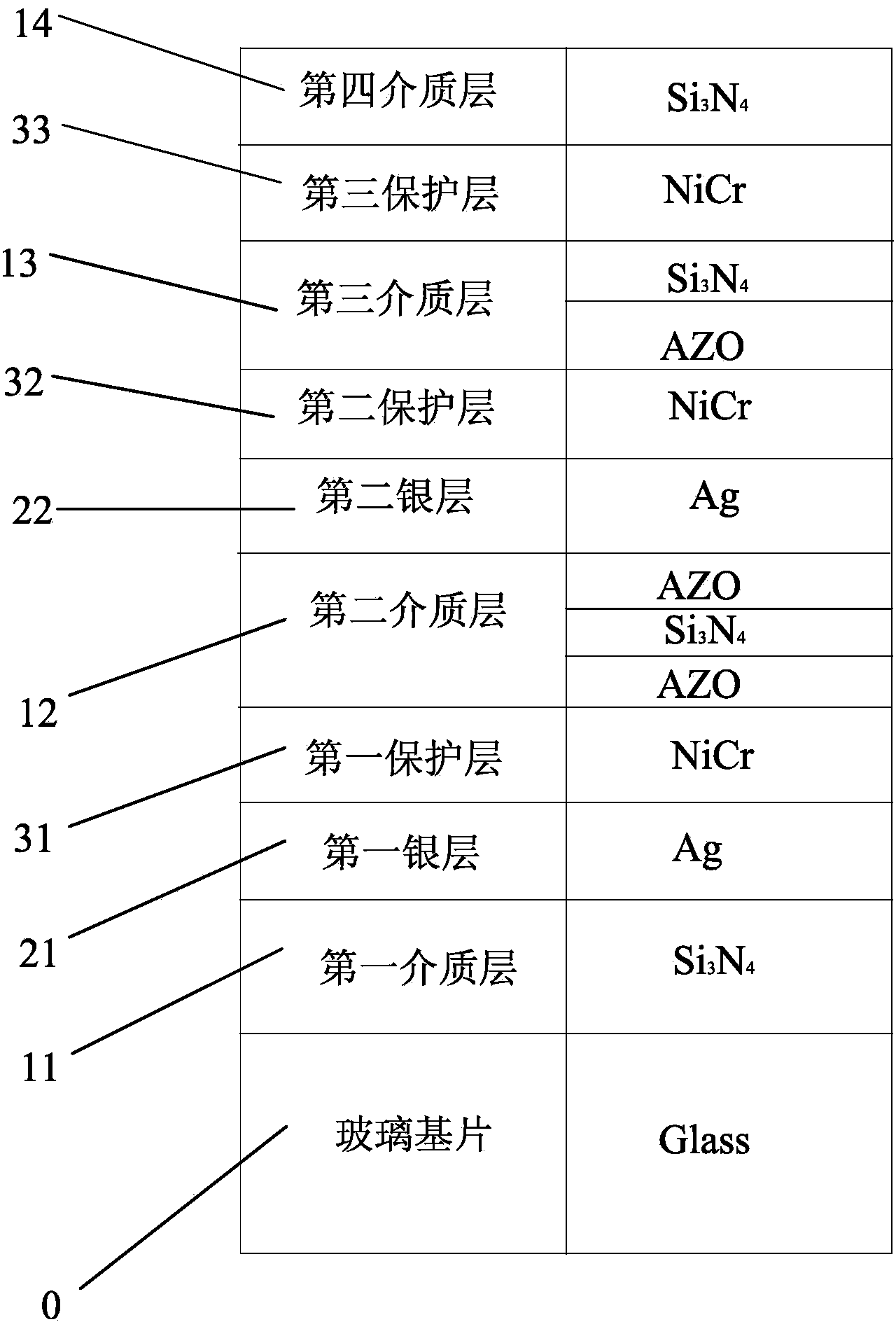
[0023] Such as figure 1 , a double-silver low-emissivity coated glass, comprising a glass substrate O and a film layer coated on the surface of the glass substrate; the film layer is sequentially provided with a thickness of 47nm from one side of the glass substrate outwards The first dielectric layer 11 with a thickness of 5 nm, the first silver layer 21 with a thickness of 5 nm, the first protective layer 31 with a thickness of 3 nm, the second dielectric layer 12 with a thickness of 67 nm, the second silver layer 22 with a thickness of 17 nm, and a thickness of 1 nm The second protective layer 32, the third dielectric layer 13 with a thickness of 31nm, the third protective layer 33 with a thickness of 3nm, and the fourth dielectric layer 14 with a thickness of 24nm, wherein the first dielectric layer 11, the second dielectric layer 12 , the third dielectric layer 13 and the fourth dielectric layer 14 are all Si 3 N 4 layer, the first protective layer 31, the second protec...
Embodiment 2
[0030] A double-silver low-emissivity coated glass, comprising a glass substrate O and a film layer coated on the surface of the glass substrate; the film layer is sequentially provided with a thickness of 53nm from one side of the glass substrate outwards The first dielectric layer 11, the first silver layer 21 with a thickness of 3nm, the first protective layer 31 with a thickness of 3nm, the second dielectric layer 12 with a thickness of 73nm, the second silver layer 22 with a thickness of 18nm, and the The second protective layer 32, the third dielectric layer 13 with a thickness of 23nm, the third protective layer 33 with a thickness of 1nm, and the fourth dielectric layer 14 with a thickness of 25nm, wherein the first dielectric layer 11 is formed from the glass substrate 0 to The outside is sequentially provided with Si with a thickness of 50nm 3 N 4 layer and an AZO layer with a thickness of 3nm, and the second dielectric layer 12 is sequentially provided with Si with...
Embodiment 3
[0036] A double-silver low-emissivity coated glass, comprising a glass substrate O and a film layer coated on the surface of the glass substrate; the film layer is sequentially provided with a thickness of 53nm from one side of the glass substrate to the outside. A dielectric layer 11, a first silver layer 21 with a thickness of 6 nm, a first protective layer 31 with a thickness of 3 nm, a second dielectric layer 12 with a thickness of 60 nm, a second silver layer 22 with a thickness of 10 nm, and a first protective layer 31 with a thickness of 5 nm. Two protective layers 32, a third dielectric layer 13 with a thickness of 37nm, a third protective layer 33 with a thickness of 1nm, and a fourth dielectric layer 14 with a thickness of 30nm, wherein the first dielectric layer 11 is Si 3 N 4 layer, and the second dielectric layer 12 is sequentially provided with an AZO layer with a thickness of 5 nm and a Si layer with a thickness of 45 nm from the glass substrate 0 to the outside...
PUM
| Property | Measurement | Unit |
|---|---|---|
| thickness | aaaaa | aaaaa |
| thickness | aaaaa | aaaaa |
| thickness | aaaaa | aaaaa |
Abstract
Description
Claims
Application Information
 - R&D
- Intellectual Property
- Life Sciences
- Materials
- Tech Scout
- Unparalleled Data Quality
- Higher Quality Content
- 60% Fewer Hallucinations
Browse by: Latest US Patents, China's latest patents, Technical Efficacy Thesaurus, Application Domain, Technology Topic, Popular Technical Reports.
© 2025 PatSnap. All rights reserved.Legal|Privacy policy|Modern Slavery Act Transparency Statement|Sitemap|About US| Contact US: help@patsnap.com


