
Once molding processing device and technology for precision optical element

A technology of precision optics and molding processing, applied in glass molding, glass remolding, manufacturing tools, etc., can solve the problems of the failure of precision optical components, increase the burden and pressure of enterprises, limit the growth and development of enterprises, etc., to avoid processing The effect of failure, promotion, smooth operation of equipment

Inactive Publication Date: 2013-10-09
雅安格纳斯光电科技有限公司
View PDF5 Cites 4 Cited by
  • Summary
  • Abstract
  • Description
  • Claims
  • Application Information

AI Technical Summary

Problems solved by technology

The finished products of precision optical components can only be obtained after the above-mentioned steps, and each link in these processes needs to be perfect to obtain the required precision optical components, and it is difficult to ensure that each step is accurate during each step It can be carried out perfectly, and because the requirements for various indicators of precision optical components are very strict, no matter which step has an error, it will lead to the failure of the production of the precision optical component, which greatly limits the improvement of product processing efficiency and greatly increases Processing costs increase the burden on enterprises
At the same time, in the production process of the product, it needs to go through multiple inspections, and the inspection method is done manually, which requires a lot of human resources to spend on various inspection levels, which further increases the burden and pressure on the enterprise, thus greatly limiting The growth of the enterprise and the development of the industry

Method used


Image

  • Once molding processing device and technology for precision optical element
  • Once molding processing device and technology for precision optical element

Examples


Embodiment 1

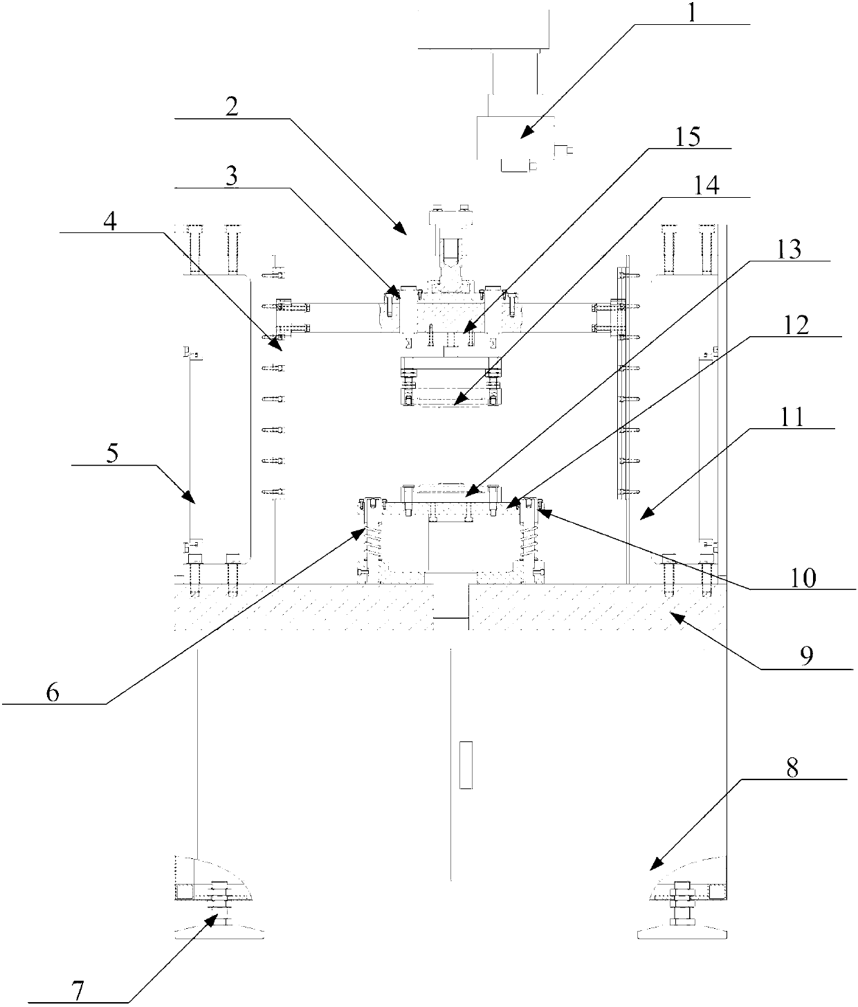
[0036] Such as figure 1 As shown, the precision optical element one-time molding processing device includes a frame 8, an adjustable support foot 7 is arranged at the lower end of the frame 8, a workbench 9 is arranged at the upper end of the frame 8, and a workbench 9 is also arranged on the workbench 9. A lower mold device and a column 11 are provided, and an upper support plate 2 is arranged on the top of the column 11. An upper mold device and a servo electric cylinder 1 are also arranged on the upper support plate 2. At the same time, the servo electric cylinder 1 is also connected There is a control cabinet.

[0037] Above-mentioned lower mold device comprises lower floating support frame 12, and this lower floating support frame 12 is provided with the support bar that is fixed on the workbench 9, and this support bar is covered with spring 6, and between the lower floating support frame 12 and the support bar A lower linear bearing 10 is provided, and a mold lower mol...


PUM


Abstract

The invention discloses a once molding processing device and technology for a precision optical element. The device comprises a rack, wherein adjustable support legs are arranged at the lower end of the rack, a workbench is arranged at the upper end of the rack and is also provided with a lower die device and uprights, and an upper support plate is arranged at the top ends of the uprights and is also provided with an upper die device and a servo electric cylinder which is connected with a control cabinet. The technology comprises the following steps of: A. design, manufacture and installation of a die; B. preparation of materials; C. profiling through warming; D. annealing; E. examination; F. trimming; G. cold machining; and H. examination. According to the device and the technology, the production processes are simplified, the possibility of errors is lowered, manpower investment is lowered, the yield and production efficiency of the finished products is greatly improved, and the cost for production is saved.

Description

technical field [0001] The invention relates to a precision optical element processing device, in particular to a precision optical element one-time molding processing device and its technology. Background technique [0002] At present, when processing precision optical components, the steps are: (1) mold design, production, installation; (2) deep-fried sticks; (3) dry cutting; (4) weight inspection; (5) grinding; (6) Weight inspection; (7) vibration grinding; (8) initial inspection; (9) heating and pressing; (10) annealing; (11) inspection; (12) milling; (13) fine grinding one side; (14) fine grinding Two sides; (15) edging; (16) polishing one side; (17) polishing two sides; (18) cleaning; (19) inspection. The finished products of precision optical components can only be obtained after the above-mentioned steps, and each link in these processes needs to be perfect to obtain the required precision optical components, and it is difficult to ensure that each step is accurate ...

Claims


Application Information

Patent Timeline
Patent Type & Authority Applications(China)
IPC IPC(8): C03B23/00
CPCY02P40/57
Inventor 王斌
Owner 雅安格纳斯光电科技有限公司
Learn More