
OLED pixel and display panel using same

A display panel and pixel technology, applied in the field of OLED pixels and display panels, can solve the problems of low luminous efficiency and color distortion, and achieve the effect of reducing the area ratio, increasing the ratio and improving the resolution.

Active Publication Date: 2013-09-25
SHANGHAI ADVANCED RES INST CHINESE ACADEMY OF SCI
View PDF4 Cites 9 Cited by
  • Summary
  • Abstract
  • Description
  • Claims
  • Application Information

AI Technical Summary

Problems solved by technology

[0008] In view of the above-mentioned shortcomings of the prior art, the purpose of the present invention is to provide an OLED pixel and a display panel using the OLED pixel, which are used to solve the problems caused by the life difference of different light-emitting materials and different color conversion materials in the prior art. The problem of color distortion is also used to solve the problem of low luminous efficiency in the prior art

Method used


Image

  • OLED pixel and display panel using same
  • OLED pixel and display panel using same
  • OLED pixel and display panel using same

Examples


Embodiment 1

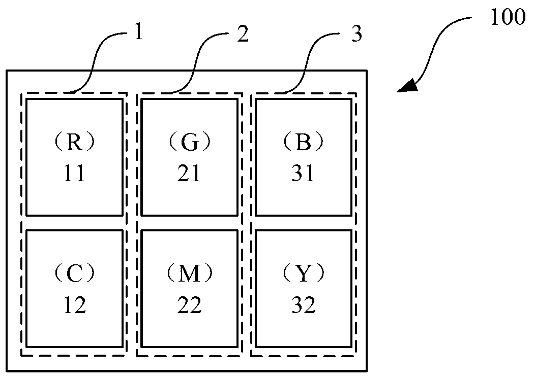
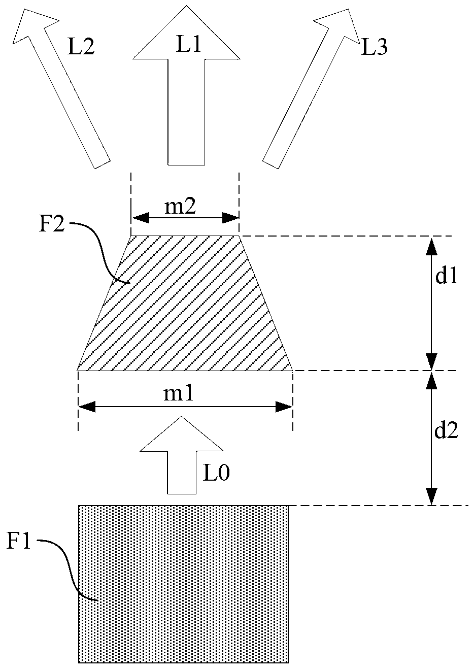
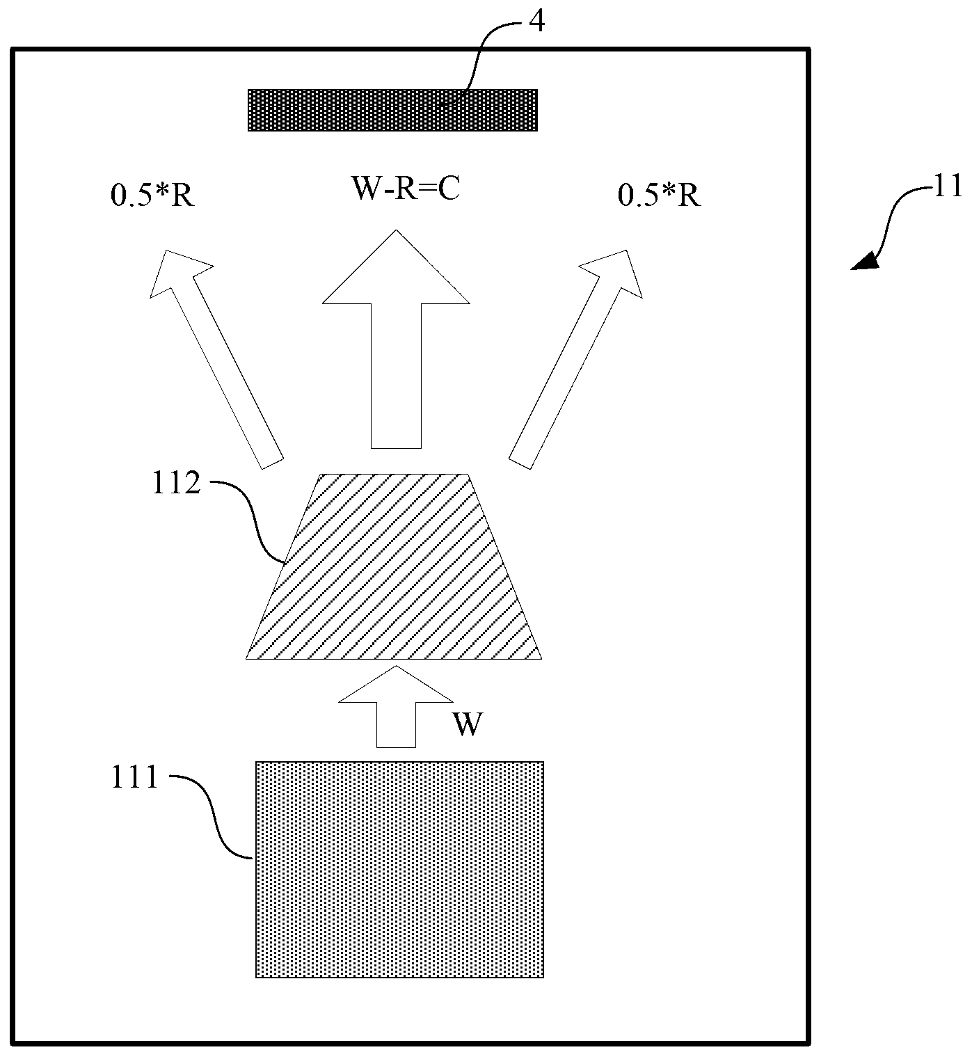
[0042] Such as Figure 1 to Figure 4 As shown, the present invention provides an OLED pixel 100 at least comprising: a first sub-pixel group 1 , a third sub-pixel group 3 and a second sub-pixel group 2 located between the first and third sub-groups. The OLED pixel 100 is rectangular, and in this embodiment, preferably, the OLED pixel 100 is square.

[0043] Wherein, each of the sub-pixel groups includes a common driving circuit (see the second embodiment for details) Figure 5 ) of the first sub-pixel and the second sub-pixel, and each of the first sub-pixel and the second sub-pixel is connected to its corresponding driving circuit, such as figure 1 As shown, the first sub-pixel group 1 includes the first sub-pixel 11 of the first sub-pixel group and the second sub-pixel 12 of the first sub-pixel group, and the second sub-pixel group 2 includes the second sub-pixel The first sub-pixel 21 of the pixel group and the second sub-pixel 22 of the second sub-pixel group, the third ...

Embodiment 2

[0084] The present invention also provides an OLED display panel, at least comprising: a plurality of OLED pixels as described in Embodiment 1, a plurality of selection lines within a group, a plurality of data lines, and a plurality of row scanning lines.


PUM


Abstract

The invention provides an OLED pixel and a display panel using the same. The OLED pixel comprises three sub-pixel groups. Each sub-pixel group comprises a first sub-pixel and a second sub-pixel, wherein the first sub-pixel and the second sub-pixel share one driving circuit, and the light emitting waveband of the first sub-pixel and the light emitting waveband of the second sub-pixel are complementary. The sum of the light emitting wavebands of the first sub-pixels of the sub-pixel groups is a white light waveband. According to the OLED pixel and the display panel using the same, the sub-pixels are formed by means of the principle of diffraction of light and the combination of white light OLED light emitting bodies, beam splitting pieces and light barriers. Due to the fact that the six kinds of sub-pixels all adopt the white light OLED light emitting bodies, the problem of chromatic aberration caused by different aging degrees of different materials is avoided. Due to the fact that three kinds of sub-pixels are additionally arranged to assist imaging processing, luminous efficiency of the OLED pixel is improved and power consumption is reduced. Due to the fact that the two sub-pixels of each sub-pixel group share one driving circuit, the distinguishability of the OLED display panel is improved.

Description

technical field [0001] The invention belongs to the field of semiconductors, and relates to a color realization method of an OLED (organic light-emitting diode), in particular to an OLED pixel and a display panel using the OLED pixel. Background technique [0002] Organic light-emitting diodes (Organic Light-Emitting Diode, OLED) can be used for flexible panels, use Wide temperature range, simple structure and manufacturing process and other excellent characteristics have attracted widespread attention and are used in flat panel display and other fields. [0003] There are three main methods used by traditional OLEDs to display color images: [0004] 1. Use different luminescent materials to achieve RGB three-color luminescence. However, the disadvantage of this method is that the luminescent materials must be optimized for different colors, and the luminescent layers of different materials have differences in service life. Different aging The degree makes the display colo...

Claims


Application Information

Patent Timeline
Patent Type & Authority Applications(China)
IPC IPC(8): H01L27/32G09G3/32G09G3/3225
Inventor 施琛汪宁汪辉章琦封松林
Owner SHANGHAI ADVANCED RES INST CHINESE ACADEMY OF SCI
Learn More