
Structure of stacking chips and method for manufacturing the same

By forming recesses and through-holes on the glass substrate for electrical connection, the problem of complex packaging structures and large area occupation of the image sensor chip and digital signal processor chip is solved, achieving space saving, process simplification and reliability improvement.

Active Publication Date: 2013-09-25
CHIPMOS TECH INC
View PDF4 Cites 12 Cited by
  • Summary
  • Abstract
  • Description
  • Claims
  • Application Information

AI Technical Summary

Problems solved by technology

The process is relatively complicated and the production time is long, and the manufacturing cost is high
In addition, the image sensor chip 11 and the digital signal processor chip 12 are arranged horizontally side by side on the substrate, occupying a large area, and the reliability of the wire bonding is not good, which is prone to the disadvantages of poor contact or poor stability.

Method used


Image

  • Structure of stacking chips and method for manufacturing the same
  • Structure of stacking chips and method for manufacturing the same
  • Structure of stacking chips and method for manufacturing the same

Examples


Embodiment Construction

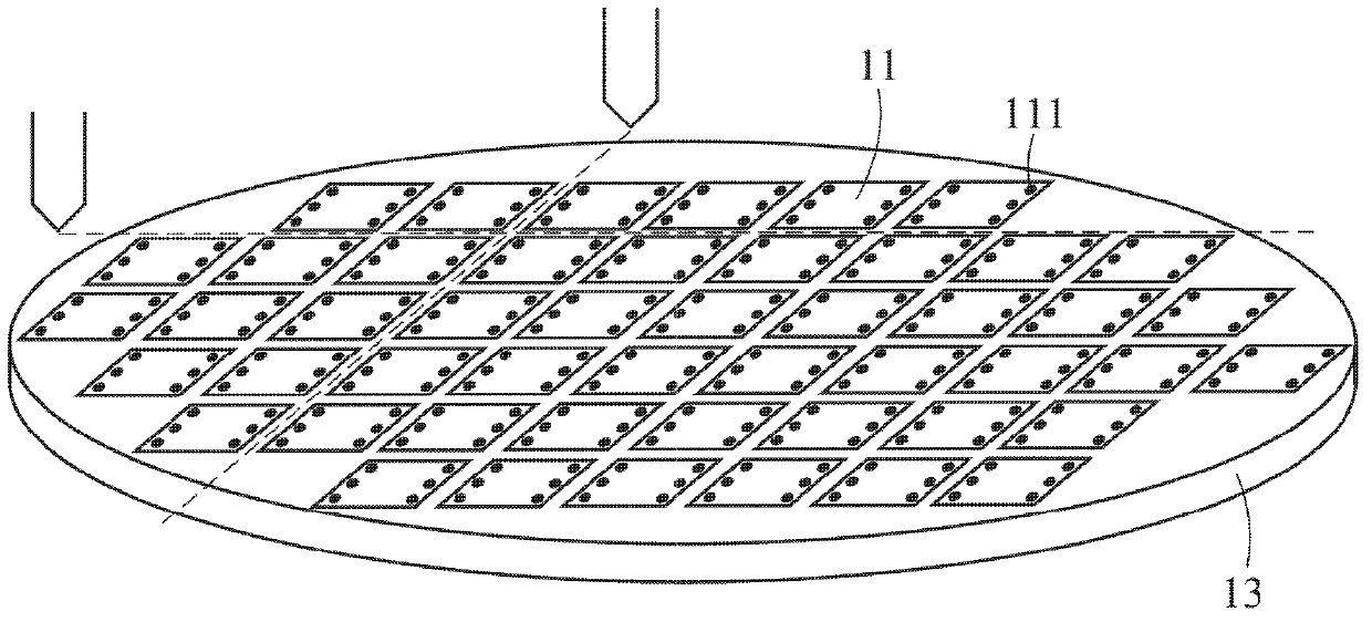
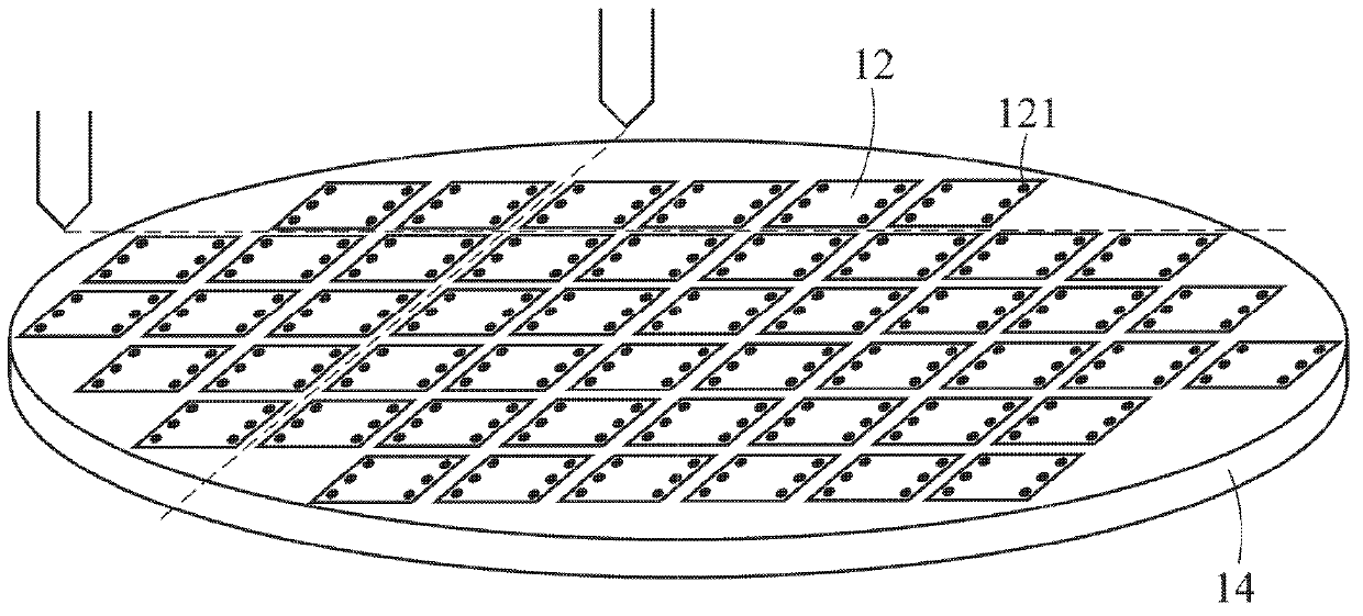
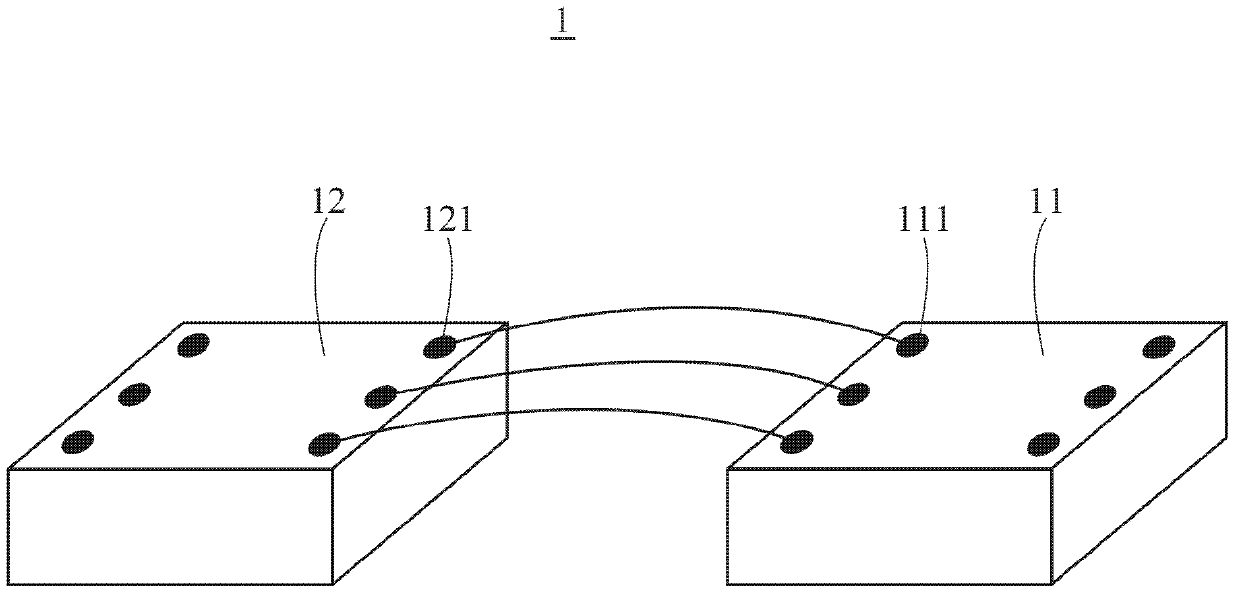
[0044] see figure 2 , is a schematic cross-sectional view of the stacked chip structure 2 according to the first embodiment of the present invention, which is a stacked structure including an optical chip module 21 and a signal processing chip module 23 .

[0045] Wherein, the signal processing chip module 23 includes a glass substrate 231 and a signal processing chip 233 , and the signal processing chip 233 is preferably a digital signal processor (DSP) chip. For the convenience of description, it is further defined that the glass substrate 231 has a first surface 231a and a second surface 231b opposite to the first surface 231a, and the glass substrate 231 is further formed with a plurality of through holes (through holes) 235, in which Metal material is plated to connect the first surface 231a and the second surface 231b.

[0046] A cavity 237 is further formed on the first surface 231 a of the glass substrate 231 for the signal processing chip 233 to be disposed in the c...


PUM


Abstract

A structure of stacking chips and a method for manufacturing the structure of stacking chips are provided. A wafer with optical chips and a glass substrate with signal processing chips are stacked with each other, and then subjected to ball mounting and die sawing to form the stacked packaging structure. The optical chips and the signal processing chips form the electrical connection on the surface of the glass substrate via the through holes thereof.

Description

technical field [0001] The present invention relates to a chip stacking structure and a manufacturing method thereof. The chip stacking structure particularly includes a stacking structure of a signal processing chip and an optical chip. Background technique [0002] With the evolution of people's living habits and the advancement of technology, image sensors have been widely used in daily life. Known image sensors include, for example, complementary metal-oxide semiconductor (complementary metal-oxide semiconductor, CMOS) image sensors, charge coupled device (charge coupled device, CCD) image sensors, and the like. Among them, CMOS image sensors have the advantages of low price and low power consumption, and are usually more suitable for low-end products; while CCD image sensors capture better image quality, and have long dominated the market for high-end image sensors. [0003] However, due to the addition of a digital signal processor (digital signal processor, DSP) chip...

Claims


Application Information

Patent Timeline
Patent Type & Authority Applications(China)
IPC IPC(8): H01L27/146H01L23/488H01L21/60
CPCH01L24/97H01L2224/48137H01L2224/48091H01L2224/49175H01L2924/00014H01L23/10H01L21/563H01L24/13H01L24/16H01L24/29H01L24/32H01L24/73H01L24/83H01L24/92H01L24/94H01L2224/131H01L2224/13139H01L2224/13144H01L2224/13147H01L2224/16235H01L2224/29011H01L2224/32052H01L2224/32225H01L2224/73104H01L2224/73204H01L2224/83191H01L2224/92125H01L2224/94H01L2224/97H01L2924/14335H01L2924/15153H01L2924/15311H01L2924/15788H01L2224/16227H10F39/026H01L2224/45099H01L2224/81H01L2924/00015H01L2924/014H01L2224/11H01L2224/83H01L2224/27H01L2924/00012H01L2924/00H01L2224/16225H10F39/811H10F39/011H01L23/00
Inventor 沈更新陈雅琪毛苡馨
Owner CHIPMOS TECH INC
Learn More