A flip-chip process of power semiconductor modules before welding

A power semiconductor, flip-chip technology, applied in semiconductor devices, semiconductor/solid-state device manufacturing, electric solid-state devices, etc., can solve the problems of electrode failure, increased assembly time, low labor productivity, etc., to improve positioning accuracy, improve Good quality and reliability, consistent product performance

Active Publication Date: 2015-11-04
LINHAI ZHIDING ELECTRONICS SCI & TECH
View PDF3 Cites 0 Cited by
  • Summary
  • Abstract
  • Description
  • Claims
  • Application Information

AI Technical Summary

Problems solved by technology

In order to insulate the die and the bottom plate, an insulating sheet or a semiconductor copper-clad ceramic substrate DBC (Direct-Bond Copper) substrate 4 should be added in between; in order to solder between layers, solder sheets should be added between each layer 6, 7, 8, 9, thereby forming up to nine layers of positive (sequential) installation process, but this positive (sequential) installation process has the following problems. First, the manufacturing of the fixing bracket is complicated, and it is difficult to fix. It is difficult to resist, and it is almost impossible to complete the assembly; second, the accuracy of the alignment position of the solder point between layers is very poor, resulting in poor device performance consistency and high defective products; third, the complexity of the assembly bracket leads to assembly The process is complicated, the assembly time is increased, the labor productivity is low, and the assembly line production cannot be realized; fourth, the lead-out electrodes cannot be directly welded to the chip, so metal filaments must be introduced for transitional connection, and the assembly cannot be completed at one time
To sum up, the method of forward (sequential) assembly of power semiconductor modules before welding cannot well solve the problem of mass production of power semiconductor modules, nor can it control product quality and product cost well.

Method used


Image

  • A flip-chip process of power semiconductor modules before welding
  • A flip-chip process of power semiconductor modules before welding

Examples


Embodiment Construction

[0028] The following are specific embodiments of the present invention and in conjunction with the accompanying drawings, the technical solutions of the present invention are further described, but the present invention is not limited to these embodiments.

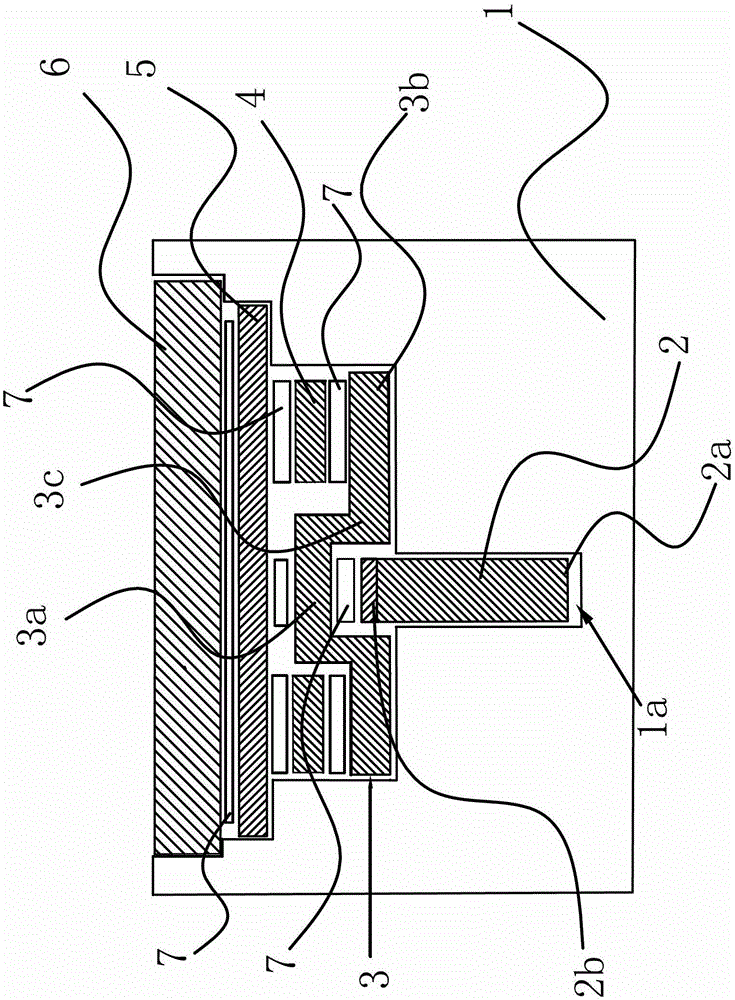
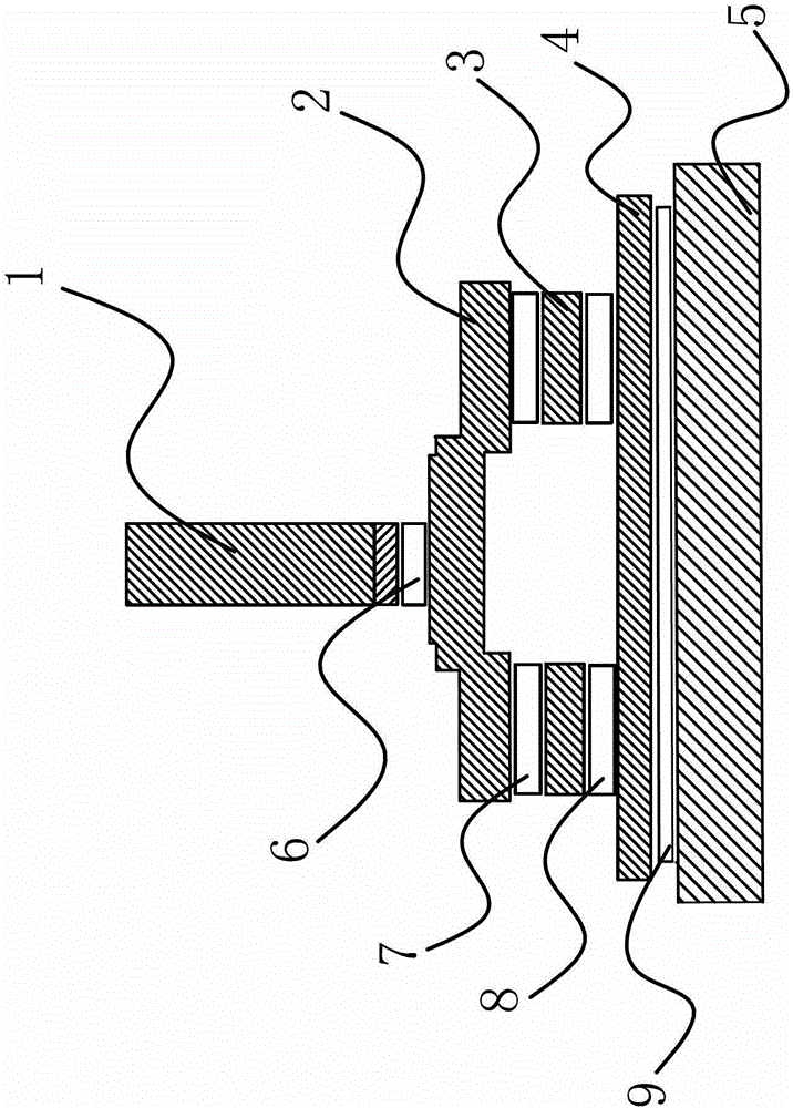
[0029] Such as figure 1 As shown, the flip-chip process of the power semiconductor module before welding, the power semiconductor module includes a base plate 6, an insulating sheet or a DBC substrate 5, a die or chip 4, an internal interconnection electrode 3 and a lead-out electrode 2, the flip-chip process The specific steps are as follows: Step 1, making a bracket 1 that has a mounting groove 1a and supports and fixes the components in the power semiconductor module through the mounting groove 1a; Step 2, placing the lead-out electrode 2 in the mounting groove 1a of the bracket 1 and For positioning and fixing, the lead-out electrode 2 includes a lead-out pole 2a for connecting to an external circuit and a welding pol...


PUM


Abstract

The invention provides a pre-welding inverse installation technology of a power semiconductor module, belonging to the technical field of semiconductor components of electrical equipment. By the adoption of the pre-welding inverse installation technology of the power semiconductor module, the problems that products manufactured by an existing technology are low in quality and high in cost are solved. The pre-welding inverse installation technology of the power semiconductor module comprises the following steps of placing a support in which an installation groove is formed on the base layer at first, placing an extraction electrode on the first layer of the installation groove, placing an intraconnection electrode on the second layer, placing a tube core or a chip on the third layer, placing an insulating strip or a DBC (Direct Bonded Copper) substrate on the fourth layer, and placing a base plate on the fifth layer, wherein components placed on all layers are positioned, supported and fixedly arranged by the support respectively. The inverse installation technology enables the production rate of the power semiconductor module to be improved, and moreover, produced products are better in quality and lower in cost.

Description

technical field [0001] The invention belongs to the technical field of power equipment semiconductor devices, and relates to a power semiconductor module flip-chip process before welding. Background technique [0002] High-power semiconductor modules need to weld the bottom plate, die or chip, and lead-out electrodes before packaging, and assemble and fix the bottom plate, die or chip, and lead-out electrodes before welding. [0003] In the prior art both at home and abroad, the positive (shun) loading process method (such as figure 2 As shown), the so-called positive (sequential) packaging process method is to place the base plate on the bottom layer 5, place the die 3 superimposed on the base plate, and then place the lead-out electrode 1 on the die. In order to insulate the die and the bottom plate, an insulating sheet or a semiconductor copper-clad ceramic substrate DBC (Direct-Bond Copper) substrate 4 should be added in between; in order to solder between layers, solde...

Claims


Application Information

Patent Timeline
Patent Type & Authority Patents(China)
IPC IPC(8): H01L21/50H01L21/58
CPCH01L24/34H01L24/33H01L2924/15747H01L2924/15787H01L2224/40137H01L2224/40H01L2924/00
Inventor 梁思平董建平
Owner LINHAI ZHIDING ELECTRONICS SCI & TECH
Why Eureka
Try Eureka